Poster Session 3

16:45 - 17:53 Wednesday, 7th July, 2021

Sessions Poster Session


16:46 - 16:47

7 Gaining meaningful statistical data on TEM specimens through automated nanoparticle workflow (APW)

Dr. Anil Yalcin
Thermo Fisher Scientific, Eindhoven, Netherlands

Abstract Text

While S/TEM imaging methods and characterization techniques give insights on specimens, acquired images intrinsically represent a limited area (due to S/TEMs being high resolution instruments) with scarce statistical input. When nanoscale statistical data is required, this is achieved through manually acquiring multiple S/TEM (spectrum) images and processing them individually, which is not an ideal workflow. Moreover, sample size is kept small (around 50 particles) due to the extent of manual operation in image acquisition and processing. 

One field requiring nanoscale statistical data is the food industry, where European Food Safety Authority (EFSA) recommended that titanium dioxide nanoparticle additives should include more statistical information (besides the current EU specifications) acquired through electron microscopy techniques [1]. EFSA recommendation has been adopted already by several research institutes. A recent publication proposes a method for quantification and size distribution of titanium dioxide nanoparticles in confectionery by means of S/TEM [2].

To eliminate manual involvement in (spectrum) image acquisition and processing, Thermo Fisher has developed an automated nanoparticle workflow (APW). With clever communication between microscope optics and stage, large area (spectrum) imaging can now be carried out in high resolution in an automated way on S/TEM. Moreover, thanks to the integrated energy dispersive x-ray spectroscopy (EDS) detectors, one can simultaneously conduct elemental analysis and acquire STEM images during APW workflow. Acquired data is processed on-the-fly, enabling immediate access to statistics and considerably reducing time to data. With the whole workflow being automated, large sample sizes can be achieved, ensuring more reliable and meaningful statistics.

As electron microscopy techniques are nowadays generating large datasets, APW will help users retrieve meaningful information on their specimens in an unattended way without any additional time for data processing. We believe that besides the food industry, APW will address numerous research fields/industries where sample statistics are of great significance, such as metals (precipitate analysis) and catalysis (correlation between particle size and surface area).

Keywords

Statistics, Automated Nanoparticle Workflow (APW), Food Additives, Precipitate Analysis, Catalysis

References

[1] Younes, M. et al. EFSA Journal, 2019, 17, 5760.

[2] Geiss, O. et al. Food Control, 2021, 120, 107550.


16:48 - 16:49

13 Building a rotational near field ptychography

Mr Yiqian Zhang
University of Sheffield, Sheffield, United Kingdom

Abstract Text

Near field Ptychography can rebuild complex 2D waves using iterative algorithms and diffraction data collected from optical microscopy systems. It demonstrates excellent phase sensitivity with a high field of view (FOV) and undemanding alignment procedures. However, Ptychography usually involves sample movement, so the quality of reconstruction and data collection time are considerably worse when the object is fluid. In this poster, I will introduce a modified method for data collection which is based on near field Ptychography. Instead of scanning the object step by step, a rotating aperture is used to introduce diversity into the ptychography process hence, the sample stays unchanged during the experiment. This idea can deliver high accuracy phase images with a small number of measured diffraction patterns, it is quick, and it can be added on very simply to an existing microscope platform.

Keywords

quantitative phase imaging, Ptychography, Near field Ptychography, Fast data collection,

References

[1]A. Maiden and J. Rodenburg, "An improved ptychographical phase retrieval algorithm for diffractive imaging", 2009.

[2]S. McDermott and A. Maiden, "Near-field ptychographic microscope for quantitative phase imaging", 2018.

[3]Y. Geng et al., "Enhanced multi-rotation computational coherent imaging based on pre-illumination and simulated annealing compensation", 2019.


16:49 - 16:50

19 Expanding Performance and Usability of High-speed / Low-dose STEM Scanning

Tiarnan Mullarkey1,2, Jonathan J.P. Peters2, Clive Downing3, Lewys Jones2,3
1Centre For Doctoral Training in the Advanced Characterisation of Materials, Dublin, Ireland. 2School of Physics, Trinity College Dublin, Dublin, Ireland. 3Advanced Microscopy Laboratory, Centre for Research on Adaptive Nanostructures and Nanodevices (CRANN), Dublin, Ireland

Abstract Text

Modern advances in scanning transmission electron microscopy (STEM), such as aberration correction, have meant that for many technologically relevant samples it is no longer our instrument that limits our resolution, but instead sample damage caused by the electron beam [1,2]. Reducing both the electron dose and the dose-rate by lowering the beam current and pixel dwell-time are key avenues to combat this which are available to all microscope operators. 

However, when imaging under these conditions, we find that artefacts such as signal streaking and detector afterglow begin to dominate our images [3]. Even in the absence of these artefacts the signal level in a single image frame is too low for the precision required in many studies, whilst navigating and focusing the image become near impossible. The problems then are severalfold; finding a way to eliminate these imaging artefacts, enabling navigating under ultra-low-dose conditions, and producing final data of a suitably high signal level.

Here we present a strategy for software and hardware retrofitting of the Gatan Digiscan to solve these issues in the following ways:

  • Using a  refinement of our previous work [4], we pulse count electrons with a FPGA to create digital images live within Digital Micrograph to eliminate the previously described artefacts.
  • Implementation of a live rolling live-average, such as those seen in SEMs, into Digital Micrograph to aid in navigating under low-dose conditions.
  • Enabling the ability to capture a continuous buffer of image frames, allowing live playback of data, including those from before the operator began recording.

The combination of the above approaches natively into Digital Micrograph creates a powerful tool where the image acquisition capabilities of the STEM are pushed to their limits. Every electron is counted in the digital signal, and with the image buffer no data is wasted. These benefits are exemplified when imaging fragile specimens as the rolling live-average eliminates the need to go to higher electron doses to find a region of interest within the sample, and live playback of frames means we may be able to capture crucial dynamic events, if not rewind to before a point where a sample becomes too damaged. These benefits will be demonstrated through comparisons of analogue and digital data, and examples where the data buffer was used to find otherwise irretrievable data.


References

[1]       R. F. Egerton, P. Li, and M. Malac, Micron 35, 399 (2004).

[2]       A. De Backer, G. T. Martinez, K. E. MacArthur, L. Jones, A. Béché, P. D. Nellist, and S. Van Aert, Ultramicroscopy 151, 56 (2015).

[3]       J. P. Buban, Q. Ramasse, B. Gipson, N. D. Browning, and H. Stahlberg, J. Electron Microsc. (Tokyo). 59, 103 (2010).

[4]       T. Mullarkey, C. Downing, and L. Jones, Microsc. Microanal. 26, 2964 (2020).


16:50 - 16:51

20 The correlation between ptychographic phase and ADF intensity: A new approach for quantitative STEM

Dr Ali Mostaed1, Prof Angus I. Kirkland1,2,3, Prof Peter Nellist1
1Department of Materials, University of Oxford, Oxford, United Kingdom. 2electron Physical Science Imaging Centre (ePSIC), Diamond Light Source, Didcot, United Kingdom. 3Rosalind Franklin Institute, Harwell Campus, Didcot, United Kingdom

Abstract Text

The abstract content is not included at the request of the author.

Keywords

Ptychography, ADF, Quantitative STEM

References

[1] T. Seki, Y. Ikuhara, N. Shibata, Ultramicroscopy 193 (2018) 118–125.

[2] L.J. Allen, A.J. D׳Alfonso, S.D. Findlay, Ultramicroscopy 151 (2015) 11–22.


16:51 - 16:52

24 Laser-free super-resolution microscopy

Dr Kirti Prakash
National Physical Laboratory, London, United Kingdom

Abstract Text

We report that high-density single-molecule super-resolution microscopy can be achieved with a conventional epifluorescence microscope setup and a Mercury arc lamp. The configuration termed as laser-free super-resolution microscopy (LFSM), is an extension of single-molecule localisation microscopy (SMLM) techniques and allows single molecules to be switched on and off (a phenomenon termed as "blinking"), detected and localised. The use of a short burst of deep blue excitation (350-380 nm) can be further used to reactivate the blinking, once the blinking process has slowed or stopped. A resolution of 90 nm is achieved on test specimens (mouse and amphibian meiotic chromosomes). Finally, we demonstrate that STED and LFSM can be performed on the same biological sample using a simple commercial mounting medium. It is hoped that this type of correlative imaging will provide a basis for a further enhanced resolution.


Uncaptioned visual

References

Prakash, Kirti. "Laser-free super-resolution microscopy." bioRxiv (121061).


16:52 - 16:53

28 Plasma FIB Spinmill for Al alloy Sample Preparation

Dr. Changrun CAI1, Mr. Haifeng Gao1, Dr. Yinghong Lin1, Dr. Erwan Sourty1, Mr. Cliff Bugge2, Miss Xiangli Zhong3
1MSD, Thermo Fisher Scientific, Shanghai, China. 2Thermo Fisher Scientific, Portland, USA. 3The University of Manchester, Manchester, United Kingdom

Abstract Text

In the present study, the low accelerating voltage Plasma Focused Ion Beam spinmill (PFIB-SM) [1–3] technique was applied for SEM-EBSD sample preparation, to replace traditional methods such as polishing and ion milling. The using of PFIB-SM made sample preparation simple, time-saving, high quality, site specific and accurate. Here we present the results of PFIB-SM procedure which was successfully applied to an as-received rolling aluminium alloy, AA6061. Applying PFIB-SM procedure at 8kV for 10 min, EBSD identification rate achieved over 95% for the alloy matrix in the periphery of a Fe particle at the rolling surface of the sample. Contamination removal was observed by 7 min PFib-SM at 2 kV. The promising low voltage applications on 3D volume microscopy is proposed for reducing high voltage ion beam damage on milled slice faces.

Preparation of high-quality samples is critical for material characterization. However, it is traditionally time consuming. An experienced researcher may spend days to prepare a high quality EBSD sample. Traditional methods, such as grinding, polishing and ion milling, may miss interested surface features, as they do not have precise position control at microscale level. In addition, the transfer from laboratory to microscope may induce contamination, damage or passivation/oxidation of sample surface, resulting in unreliable characterization results. The application of PFIB-SM could potentially solve these problems. From the aspect of aluminium alloy, the presence of Fe-containing intermetallic particles in the alloys may significantly influence the quality of surface finishing treatment, such as anodizing for corrosion protection [4–9]. However, the local grain structure in the periphery of Fe-containing intermetallic particles at rolling surface has not been characterized by EBSD, largely due to the limitation of sample preparation methods.

The PFIB-SM was performed by Xe+ ion beam scanning on a sample surface with 360°periodic stage rotation, in order to treat the sample homogenously and avoid the PFIB-SM inducing tomography changing, as shown in Figure 1. After 10 min of PFib-SM procedure at 8kV, the EBSD result from the spinmill achieved over 95% identification rate, and the grain orientation and small size grains (several hundred nanometers) were successfully characterized, as shown in Figure 2 (c). These microstructure features were kept intact with minimal removal of the materials by the in-situ SEM observation during PFIB-SM, as the comparison between Figure 2 (a) and (b). In addition, Figure 3 shows the high efficiency of 2 kV PFIB-SM for contamination cleaning. The evolution from Figure 3 (a) to (c) shows that most of contamination was removed and the microstructure was kept intact by 7 min of PFIB-SM procedure. Figure 3 (d) is the BSE micrograph of the rectangle Figure 3 (c) region, showing the clear overall microstructure features of the rolling surface.

In conclusion, the present work shows PFIB-SM is a promising sample preparation procedure for SEM-EBSD sample preparation. The micrographs of rolling surface AA6061 are given as the illustration of PFIB-SM application. In addition, it is reasonable to suggest that PFIB-SM also can increase the quality of pretreated sample and avoid the contamination during sample transfer from laboratory to microscope. It also has great potential to be used as 3D/EBSD sample preparation and analyzing method if the sample stage can be progressively raised up. Low voltage milling has great potential on minimizing high voltage induced sample surface damage.

Uncaptioned visual

Figure 1. The IR photograph of PFib-SM set up.

Uncaptioned visual

Figure 2. (a): the SEM CBS A+B 5kV 1.6 nA micrograph of an Fe-containing particle before 8 kV PFib-SM; (b) the SEM CBS A+B 5kV 1.6 nA micrograph of the same Fe-containing particle after 10 min 8kV PFib-SM and (c): the corresponding EBSD All Euler of alloy matrix in the periphery of the particle in (b).

Uncaptioned visual

Figure 3. (a): the SEM ETD-SE 5kV 1.6 nA micrograph of the as-received rolling surface before 2kV PFib-SM; (b): SEM ETD-SE 5kV 1.6 nA micrograph of the as-received rolling surface after 5 min 2kV PFib-SM; (c): SEM ETD-SE 5kV 1.6 nA micrograph of the as-received rolling surface after 7 min 2kV PFib-SM and (d): the SEM CBS A+B 5kV 1.6 nA micrograph of the as-received rolling surface after 7 min 2kV PFib-SM, showing clear surface structure.


Keywords

Plasma focus ion beam (PFIB); Spinmill; Sample preparation; EBSD; aluminium alloy; rolling surface; 3D/EBSD; volume characterisation

References

[1]        Winiarski B. Plasma FIB Spin Milling Accelerates Battery Research. Microsc Microanal 2020;26:2226–7. https://doi.org/10.1017/S1431927620020863.

[2]        Winiarski B, Rue C, Withers PJ. Plasma FIB Spin Milling for 3D Residual Stress Measurements. Microsc Microanal 2019;25:882–3. https://doi.org/10.1017/s1431927619005142.

[3]        Winiarski B, Rue C, Withers PJ. Plasma FIB Spin Milling for Large Volume Serial Sectioning Tomography. Microsc Microanal 2019;25:350–1. https://doi.org/10.1017/s1431927619002484.

[4]        Saenz de Miera M, Curioni M, Skeldon P, Thompson GE. The behaviour of second phase particles during anodizing of aluminium alloys. Corros Sci 2010;52:2489–97. https://doi.org/10.1016/j.corsci.2010.03.029.

[5]        Ma Y, Zhou X, Thompson GE, Curioni M, Zhong X, Koroleva E, et al. Discontinuities in the porous anodic film formed on AA2099-T8 aluminium alloy. Corros Sci 2011;53:4141–51. https://doi.org/10.1016/j.corsci.2011.08.023.

[6]        Veys-Renaux D, Chahboun N, Rocca E. Anodizing of multiphase aluminium alloys in sulfuric acid: in-situ electrochemical behaviour and oxide properties. Electrochim Acta 2016;211:1056–65. https://doi.org/10.1016/j.electacta.2016.06.131.

[7]        Wu H, Ma Y, Huang W, Zhou X, Li K, Liao Y, et al. Effect of Iron-Containing Intermetallic Particles on Film Structure and Corrosion Resistance of Anodized AA2099 Alloy. J Electrochem Soc 2018;165:C573–81. https://doi.org/10.1149/2.1361809jes.

[8]        Zhang F, Nilsson J-O, Pan J. In Situ and Operando AFM and EIS Studies of Anodization of Al 6060: Influence of Intermetallic Particles. J Electrochem Soc 2016;163:C609–18. https://doi.org/10.1149/2.0061610jes.

[9]          Jin Z, Cai C, Hashimoto T, Yuan Y, Kang DH, Hunter J, et al. The behaviour of iron-containing intermetallic particles in aluminium alloys in alkaline solution. Corros Sci 2021;179:109134. https://doi.org/10.1016/j.corsci.2020.109134.


16:53 - 16:54

34 Phasing Out Fluorescence: Quantifying Mitosis Label-free

Dr Meetal Solanki1, Dr Rebecca Charlton1, Dr Karen Hogg2
1Phasefocus, Sheffield, United Kingdom. 2University of York, York, United Kingdom

Abstract Text

Uncaptioned visual

Mitosis is a crucial biological process that takes place in all eukaryotic cells and involves the equal segregation and division of a parent cell into two genetically identical daughter cells. This is distinguished by a highly regulated reorganisation of cell components [1]. Changes to the cell cycle, e.g. in senescence, where there is irreversible arrest of cell proliferation, has been shown to lead to aging and age-related disease [2]. By contrast, uncontrollable cell division is a hallmark of cancer and is characterised by abnormal mitosis. Subsequently, several mitotic inhibitors have been used successfully as anti-cancer drugs [3].

The fungal toxin, cytochalasin D is used as a cytotoxic agent in cancer therapy as it disrupts actin polymerisation and activates p53 independent pathways, causing arrest of the cell cycle at the G1-S phase transition. Nocodazole, another anti-cancer drug, works by impeding the formation of the mitotic spindle and cytokinesis. This arrests cells at a slightly different part of the cell cycle, blocking cells in mitosis [7]. Both these effects can result in inhibition of cellular processes such as cell division [4,5].

Current methods that exist to measure mitosis usually rely on the use of fluorescence markers, and relatively high light levels, which can ultimately perturb the natural function of cells [6]. Therefore, there is a need for a label-free technique that can reliably identify mitotic cells. Ptychography, a quantitative phase imaging (QPI) technique, produces high contrast images without the need for fluorescent labels. The consistent and enhanced contrast enables automatic segmentation and tracking of individual cells, as well as a quantitative measure of the single-cell phenotypic behaviour of whole populations. In this study we used a Livecyte system [8] to identify label free, unique phase signatures that indicate when a single cell is undergoing mitosis. A mitotic event is clearly distinguishable as the cell adopts a more spherical morphology with a greater optical thickness than resting cells.

The aim of this study was to measure and contrast the changes in mitosis between different concentrations of cytochalasin D and nocodazole as compared to untreated cells. MBA-MB-231 cells Hela cells were seeded at 10,000 cells per well in a 96 well plate and allowed to adhere for approximately 24 hours before being preincubated with a range of concentrations of cytochalasin D and nocodazole and imaging.

Using Livecyte’s label-free QPI mode and in-built Analyse software, metrics derived from the Mitosis Dashboard were compared for the different conditions.  It revealed a dose dependant decrease in the number of mitotic events and thus proliferation in both cytochalasin D and nocodazole. It was also possible to distinguish where in the cell cycle these cells may have been arrested, notably through mitotic time values. Cytochalasin D treatment caused no difference in mitotic time indicating that cells underwent cell cycle arrest before mitosis. In contrast nocodazole increased the mitotic time in a dose dependant manner suggesting a block in the cell cycle at mitosis.

These observations were in line with those reported in the literature and reinforced the known mechanisms of both drugs giving more in depth information on the precise mechanism of action between these two cell cycle inhibitors.


Keywords

label-free

phase

QPI 

mitosis

cell cycle

References

  1. Ferreira, L.T., Figueiredo, A.C., Orr, B., Lopes, D. and Maiato, H., 2018. Dissecting the role of the tubulin code in mitosis. Methods in cell biology, 144, pp.33-74.
  2. Childs, B.G., Durik, M., Baker, D.J. and Van Deursen, J.M., 2015. Cellular senescence in aging and age-related disease: from mechanisms to therapy. Nature medicine, 21(12), pp.1424-1435.
  3. H. Schatten, 2013. Mitosis. Brenner's Encyclopedia of Genetics (Second Edition), pp.448-451
  4. Trendowski M., 2015. Using cytochalasins to improve current chemotherapeutics. Anticancer Agents Med Chem., 15(3). pp 327-33.
  5. Rubtsova S.N. et al., 1998. Disruption of actin microfilaments by cytochalasin D leads to activation of p53. FEBS Lett., 430(3). pp 353-7.
  6. Sivakumar, S., Daum, J.R. and Gorbsky, G.J., 2014. Live-cell fluorescence imaging for phenotypic analysis of mitosis. In Cell Cycle Control (pp. 549-562). Humana Press, New York, NY.
  7. Kuhn, M., 1998. The microtubule depolymerizing drugs nocodazole and colchicine inhibit the uptake of Listeria monocytogenes by P388D1 macrophages. FEMS microbiology letters, 160(1), pp.87-90.
  8. Livecyte Kinetic Cytometer, from Phasefocus, UK

16:54 - 16:55

35 High resolution imaging and spectroscopy of interfaces in solid-state Li-ion batteries

Ms. Ruomu Zhang1, Dr. Weixin Song1,2, Prof. Peter Bruce1,2,3, Prof. Peter Nellist1
1University of Oxford, Oxford, United Kingdom. 2The Faraday Institution, Didcot, United Kingdom. 3The Henry Royce Institute, Oxford, United Kingdom

Abstract Text

Summary: Solid-state electrolyte (SSE) Argyrodite Li6PS5Cl and Ni-rich cathode material LiNi0.6Mn0.2Co0.2O (NMC622) have great potential in future battery technologies benefitting from high energy density and improved operational safety. However, they currently suffer from rapid capacity fading issues due to the side reaction at the SSE/cathode interface. In this work, we use simultaneous annular dark field (ADF)/energy dispersive X-ray spectroscopy (EDX)/electron energy loss spectroscopy (EELS) in scanning transmission electron microscopy (STEM) to identify the changes of microstructure, chemical homogeneity and oxidation states at the NMC622/Argyrodite interface upon spontaneous reaction. Compared to the pristine NMC622, no obvious changes are observed in structure or chemical homogeneity, while the Ni content in NMC622 has been partially oxidised by Argyrodite. HRTEM images of Argyrodite reveal that amorphisation is the primary effect of beam damage which needs to be differentiated from cycling decomposition.


Solid-state lithium-ion batteries (SSLIBs) are promising next-generation energy storage systems, owing to their significantly improved safety while still maintaining high energy density compared to conventional liquid electrolyte system lithium-ion batteries. [1] However, the capacity fading and open-circuit voltage hysteresis issues need to be resolved before commercialization. Previous studies have suggested that these losses are closely related to the side reactions at the SSE/cathode interface [2]. To gain insights into the origin of degradation and failure mechanisms in SSLIBs, the structure and composition changes of SSE/cathode interphase will be comprehensively studied in this work.


STEM is one of the most widely used atomic-scale characterisation technique. Atomic position imaging, elemental mapping and electronic structure information can be simultaneously acquired with ADF, EDX and EELS detectors. In this work, we applied ADF/EDX/EELS to study the interface between cathode material NMC622 and SSE Argyrodite Li6PS5Cl before/after cycling. Moreover, to distinguish the decomposition changes from beam damage and cycling, the pristine form of argyrodite is examined in TEM for diffraction pattern evolution upon electron beam exposure.


Atomic-resolution HRTEM images of Argyrodite (Fig.1) have been successfully acquired and the crystallites have grain size of 20-30nm while an amorphous phase is also present. In the interface study, EDX elemental mapping (Fig.2) identifies an interface between NMC622 and Argyrodite. ADF images provide structural information, while EEL spectra reveal the oxidation state at high spatial resolution simultaneously. The oxidation state is determined by white-line intensity ratio L3/L2, and L3/Lmapping will be discussed in the presentation.


It is observed in TEM that the primary effect of beam damage is amorphisation. Compared to the pristine structure, NMC622 is partially oxidised when in contact with Argyrodite due to the spontaneous reaction at SSE/cathode interface. With the comprehensive analysis of the microstructure and chemistry of SSE/cathode interphase by using ADF/EDX/EELS in STEM, our work can provide a guide for future materials selection in SSLIBs by correlating the microstructure and composition with electrochemical performance.

Uncaptioned visual


Uncaptioned visual

Keywords

Solid-state Li ion batteries, Scanning transmission electron microscopy, Solid-state electrolyte/cathode interface

References

[1] N. Naoki et al. Mater. Today 18.5 (2015): 252-264

[2] A. Jeremie et al. Chem. Mater. 29.9 (2017): 3883-3890

[3] The authors acknowledge use of characterization facilities within the David Cockayne Centre for Electron Microscopy, Department of Materials, University of Oxford and in particular the Faraday Institution (FIRG007, FIRG008), the EPSRC (EP/K040375/1 “South of England Analytical Electron Microscope”) and additional instrument provision from the Henry Royce Institute (Grant reference EP/R010145/1).


16:55 - 16:56

36 Quantifying Macrophage Phagocytosis of Bioparticles

Dr Meetal Solanki1, Dr Rebecca Charlton1, Dr Karen Hogg2
1Phasefocus, Sheffield, United Kingdom. 2University of York, York, United Kingdom

Abstract Text

Uncaptioned visual

Phagocytosis is the process by which a cell (e.g. macrophage, neutrophil or dendritic cell) engulfs pathogenic or foreign particles, giving rise to an internal compartment called the phagosome.  It is one of the main mechanisms of the innate immune system and a primary response to infection [1].

To understand the regulation of phagocytosis, and the impact that the cellular environment has on phagocytosis, particle engulfment must be quantified. Traditionally, this has been challenging but the use of fluorescent bioparticles combined with recent developments in real-time fluorescence microscopy has enabled measurement of total fluorescence intensity to quantify macrophage phagocytosis [2,3]. However, there are drawbacks with live fluorescence microscopy; for instance, phototoxicity is frequently encountered which can impair sample physiology, and even lead to cell death [4]. Furthermore, fluorescence microscopy analysis typically quantifies total fluorescence intensity which can be misleading and inhibits the study of population heterogeneity.

The aim of this study was to quantify phagocytosis of bioparticles by a RAW 264.7 macrophage-like cell line in a manner that both reduced phototoxic effects and reliably quantified cell fluorescence. In addition, as phagocytosis involves the actin-driven internalisation of particles, we sought to monitor the dose-response of the actin inhibitor cytochalasin D on phagocyte behaviour.

RAW 264.7 cells were seeded at 10,000 cells per well and allowed to adhere for approximately 24 hours. Cells were then incubated with pHrodo green E. coli bioparticles, which only fluoresce in the acidic environment of the phagosome and concentrations of cytochalasin D (10µM - 1nM). Label-free quantitative phase imaging, with a Livecyte Kinetic Cytometer [5], was used with intermittent fluorescence to automatically track cells over time and measure fluorescence periodically; this enabled investigation of phagocytosis whilst substantially reducing phototoxicity effects. The high contrast label-free images produced by Livecyte facilitated robust segmentation of cells and therefore phagocytosis activity could be quantified reliably by measuring individual cell fluorescence.

Through analysis of outputs generated by Livecyte’s Fluorescence Dashboard, a dose-dependent reduction in the median fluorescence intensity of the cells, therefore reduction in cell phagocytosis, with cytochalasin D treatment was determined. In addition, by analysing the cell fluorescence intensity and cell count, it was observed that the phagocytes were at their most active after 8 hours. 

This data suggests cytochalasin adversely affects phagocytosis of bioparticles possibly though inhibiting the actin machinery needed by macrophages to internalize foreign particles. It also utilizes single-cell segmentation algorithms and time-lapse imaging to give a reliable reading into fluorescence intensity per cell and further insight into differences between phagocytic activity throughout the experiment without causing phototoxicity.


Keywords

Phagocytosis

Fluorescence

Phase

QPI

Single-cell segmentation

Time-lapse imaging

References

  1. Uribe-Querol & Rosales, 2017. Control of Phagocytosis by Microbial Pathogens. Front Immunol. 8. 1368.
  2. Kapellos, Taylor, Lee, Cowley, James, Iqbal and Greaves, 2016. A novel real time Imaging platform to quantify macophage phagocytosis. Biochem. Pharmacol. 116. 107-119.
  3. Life Technologies, 2013. pHrodoTM Red and Green BioParticles® Conjugates for Phagocytosis. 1-6.
  4. Icha, Weber, Waters and Norden, 2017. Phototoxicity in live fluorescence microscopy, and how to avoid it. Bioessays. 39(8).
  5. Livecyte available from Phasefocus, UK.

16:56 - 16:57

41 Super-resolution microscopy of macrophage adhesion and migration

Dr Liisa Hirvonen, A/Prof Fiona Pixley
The University of Western Australia, Perth, Australia

Abstract Text

Summary


Migratory macrophages play critical roles in tissue development, homeostasis and disease so it is important to understand how their migration machinery is regulated. Following the determination of up- and downregulated gene expression in macrophage differentiation [1], we have employed SIM and STORM super-resolution techniques to explore how the distribution of these proteins changes during differentiation from immature to mature macrophages.


Introduction


Macrophages (Mφ) are a critical component of the human immune system. These cells are found in all tissues of the human body where they work to ensure that their host tissues develop and function normally. Mφ are able to move through the extracellular matrix (ECM) and are unusual cells in that they can change their mode of migration according to matrix density. Despite the importance of these migratory Mφ, little is known about the regulation of their motility machinery.

Mφ differentiate from their bone marrow-derived precursor cells under the influence of the primary Mφ growth factor, CSF-1 [2]. As part of this maturation process, CSF-1 regulates the expression of many genes controlling motility [2,3]. We have recently discovered that expression of the majority of genes regulating adhesion, actin cytoskeletal remodelling and matrix degradation changes as Mφ differentiate from non-adherent precursor cells to mature Mφ [1], however the role of individual core motility proteins in maturing migratory Mφ remains poorly understood.

We have previously used conventional confocal microscopy to examine the subcellular distribution of the motility regulating proteins [4,5]; however, lack of resolution prevented us from pinpointing the exact subcellular location of each protein. In this work, we use both fixed and live-cell cutting edge super-resolution microscopy techniques SIM and STORM/PALM in with innovative image analysis methods to map the subcellular localisation of core motility proteins.


Methods


Bone marrow-derived macrophages were seeded onto fibronectin-coated coverslips or Cy3-labelled gelatin coated coverslip-bottom dishes with CSF-1, then fixed and permeabilized as described previously [6]. For SIM imaging, actin was stained with Alexa568-phalloidin and adhesion structures with an anti-phosphopaxillin, anti-paxillin or anti-leupaxin antibody to identify focal complexes and point contacts [3]. The samples were mounted in Prolong Diamond with DAPI and imaged on a Nikon SIM Ti2 microscope with a Nikon SR Apo TIRF 100x NA1.49 oil immersion objective. For STORM imaging, cell lines with mEOS3.2 labels were created as described previously [7]. Actin was labelled with iFluor647-phalloidin (Abcam) and the medium was changed to TN buffer [8] with 50 mM MEA before the samples were imaged with Nikon N-STORM microscope with a HP Apo TIRF 100x 1.49NA oil immersion objective.


Results and discussion


3D SIM was used to examine the adhesions in immature and mature Mφ (Fig. 1A,B). Mφ form adhesion and actin cytoskeletal structures that are quite different from those seen in less motile cells or other immune cells [3], consisting of very small peripheral focal complexes and tiny ventral surface point contacts which are too small to anchor thick actin stress fibres that are found in other cells such as fibroblasts and other mesenchymal cells. It is thought that this combination of countless tiny adhesions and lack of a more rigid actin cytoskeleton allows Mφ to move more quickly and nimbly than other mesenchymal cells [3]. Mφ also form podosomes, which are actin-rich adhesion structures that degrade ECM [3]. Mφ refine their adhesion structures as they differentiate from immature poorly spread Mφ to mature well spread Mφ. Notably, mature Mφ form more point contacts with fewer focal complexes (Fig. 1A), and more podosomes, which are usually organised into matrix degrading circular rosettes (Fig. 1B). Functionally this translates into striking increases in motility and matrix degradation (Fig. 1C,D).


While SIM can provide resolution of about 100 nm, STORM can increase this further to a few tens of nm. We have used STORM to visualise podosomes in primary Mφ (Fig. 1E) and a human Mφ-like cell line, THP-1 (Fig. 1F) [9]. The increased ability of STORM to discern fine subcellular detail is clear in comparison to wide-field fluorescent images. We have used STORM to clearly demonstrate discrete paxillin rings surrounding actin cores (Fig. 1F), and are now extending this work to other adhesion proteins.


Conclusion


SIM and STORM are able to unravel the differences between immature and mature Mφ on a scale never seen before, and determine the exact subcellular location of fluorescently labelled motility- and adhesion-related proteins. This will help in deciphering the roles of up- and downregulated proteins in macrophage function. In further work, we plan to perturb the expression (by siRNA technology) or function (by the use of inhibitors) of these proteins, and to characterise their roles in Mφ adhesion and migration.[10] 


Uncaptioned visual

Figure 1. (A) Mφ stained for adhesions (green) and actin cytoskeleton (red) imaged by SIM. (B) SIM images of Mφ degrading gelatin (red), stained for actin (green) and nuclei (blue). Arrows show matrix-degrading rosettes. (C) Analysis of Mφ motility and (D) matrix degradation. (E) STORM and wide-field images of the actin cytoskeleton of mouse Mφ, and (F) two colour STORM and wide-field images of podosomes in a THP-1 cell showing paxillin (green) and actin (red).

Keywords

SIM, STORM, adhesion, macrophage, podosome


References

[1] Murrey, M. W., Steer, J. H., Greenland, E. L., Proudfoot, J. M., Joyce, D. A., and Pixley, F. J. “Adhesion, motility and matrix degrading gene expression changes in CSF-1-induced mouse macrophage differentiation”, J Cell Sci, in press, doi: 10.1242/jcs.232405, 2020.


[2] Mouchemore, K. A. and Pixley, F. J. “CSF-1 signaling in macrophages: pleiotrophy through phosphotyrosine-based signaling pathways”, Crit Rev Clin Lab Sci 49:49, 2012.


[3] Pixley, F. J. “Macrophage migration and its regulation by CSF-1”, Int J Cell Biol,

doi:10.1155/2012/501962, 2012.


[4] Owen, K. A., Pixley, F. J., Thomas, K. S., Vicente-Manzanares, M., Ray, B. J., Horwitz, A. J., Parsons, J. T., Beggs, H. E., Stanley, E. R., and Bouton, A. H. “Regulation of lamellipodial persistence, adhesion turnover, and motility in macrophages by focal adhesion kinase”, J Cell Biol. 179:1275, 2007.


[5] Pixley, F. J., Lee, P. S., Condeelis, J. S., and Stanley, E. R. “Protein tyrosine phosphatase φ regulates paxillin tyrosine phosphorylation and mediates colony-stimulating factor 1-induced morphological changes in macrophages”, Mol Cell Biol 21:1795, 2001.


[6] Dwyer, A. R., Mouchemore, K. A., Steer, J. H., Sunderland, A. J., Sampaio, N. G., Greenland, E. L., Joyce, D. A., and Pixley, F. J. “Src family kinase expression and subcellular localization in macrophages: implications for their role in CSF-1-induced macrophage migration”, J Leukoc Biol 100:163, 2016.


[7] Marsh, R. J., Pfisterer, K., Bennett, P., Hirvonen, L. M., Gautel, M., Jones, G. E., and Cox, S. “Artefact-free high density localisation microscopy”, Nat Methods, 15:689, 2018.


[8] Hirvonen, L. M. and Cox, S. “STORM without enzymatic oxygen scavenging for correlative atomic force and fluorescence superresolution microscopy”, Methods Appl Fluores, 6:045002, 2018.


[9] Hirvonen, L. M., Marsh, R. J., Jones, G. E., and Cox, S. “Combined AFM and super-resolution localisation microscopy: Investigating the structure and dynamics of podosomes”, Eur J Cell Biol, 99:151106, 2020.


[10] FJP gratefully acknowledges funding from the Cancer Council of Western Australia (APP1078830 and APP1122300). This work was performed at the facilities of Microscopy Australia at the Centre for Microscopy, Characterisation & Analysis (CMCA), The University of Western Australia, funded by the University, State and Commonwealth Governments.


16:57 - 16:58

47 The Applications of Fast Electron Detectors and 4D -STEM Imaging for Understanding Structural Changes in Li-ion Cathode Systems.

Ms Emma Hedley1, Dr Weixin Song1,2, Dr Emanuela Liberti1,3,4, Prof. Peter Bruce1,2,5,6, Prof. Peter Nellist1
1Department of Materials, University of Oxford, Oxford, United Kingdom. 2The Faraday Institution, Didcot, United Kingdom. 3electron Physical Sciences Imaging Centre (ePSIC), Diamond Light Source, Didcot, United Kingdom. 4Rosiland Franklin Institute, Didcot, United Kingdom. 5Department of Chemistry, University of Oxford, Oxford, United Kingdom. 6The Henry Royce Institute, Oxford, United Kingdom

Abstract Text


In this study we aim to demonstrate how 4D-STEM techniques can be applied in the context of understanding the degradation issues which surround the cathode component of Li-ion batteries.  Modern pixelated detectors are capable of read-out speeds up to several thousand frames per second and capable of detecting single electrons, helping to mitigate concerns surrounding beam damage 1.

Li-ion batteries have emerged as important in the development electric transport methods and electronic devices. Many of the questions surrounding battery materials relate to changes in the atomic structure which occur due to cycling. The flexibility of 4D-STEM allows techniques such as ptychography which are sensitive to the low atomic number species to be performed while also enabling virtual imaging as well as many other techniques which can reveal atomic resolution information on these materials.

The cathode is generally considered an important limiting factor in Li-ion batteries 2. Li-rich NMC’s are the state of the art in high energy density cathodes however they have been slow to commercialisation due to significant issues surrounding voltage hysteresis and capacity fade 2. An essential step in resolving these issues is developing an understanding of the structural changes which occur during cycling. In this study we examine Na0.6[Li0.2Mn0.8]O2 and Na0.75[Li0.25Mn0.75]O2 which contain only a single transition metal but are ideal to quantify the underlying mechanisms surrounding the relationship between voltage hysteresis and the superstructure ordering 3.

These materials are inherently beam sensitive, making careful consideration of the dose essential. Ptychography is a dose-efficient method which can be used for phase imaging and can be enhanced by the simultaneous acquisition of ADF images 4, as seen in figure 1.  In addition to increasing the dose efficiency simultaneous ADF images present a compelling opportunity to extract quantitative information such as has been done in previous work by De Backer et al. on atom counting methods 5.

Disordered rocksalts, such as LiMnO2, are proposed as a solution to overcome structural changes in layered cathodes but these also suffer from a sharp initial capacity fading 6. Disordered rocksalts consist of a rocksalt structure with an anion lattice of oxygen - often partially replaced with fluorine – and a cation lattice of lithium and manganese which is primarily disordered. There has been many reports on the importance of medium range order within the cation lattice on the percolation network which governs the Li-ion transport 7, despite this the length scale of the ordering is not fully understood. Fluctuation electron microscopy (FEM) is able to analyse the order on this length scale (1-4nm) and is highly sensitive to 4-body correlations 8.  Using the pencil beam mode we have used nanobeam electron diffraction (NBED) to obtain diffraction patterns probing the medium range ordering. We propose to use FEM to understand this ordering and to examine how the ordering can change with cycling.

Low-dose ptychographic reconstructions have been obtained on the honeycomb and ribbon ordered, Na0.75[Li0.25Mn0.75]O.and Na0.6[Li0.2Mn0.8]O2 respectively, an example of which is shown in figure 1. These will be presented alongside our proposed quantification methods based on using the simultaneous ADF. In addition to this our initial results of NBED experiments on pristine and cycle LiMnO2 shows promising initial results which will be discussed. These significant material results will be discussed in the context of minimising beam damage by applying advances in detector technology.


Uncaptioned visual

Figure 1:a) Simultaneous ADF acquired alongside 4D-STEM data used to form b)   synthetic dark field image by virtual imaging and c) to reconstruct the phase using the single-side band method. Images acquired on JOEL ARM200Fat 200kV using pn-ccd.

These highly beam sensitive materials push the boundaries of low-dose 4D-STEM allowing us to demonstrate the capabilities of improved detector technologies and faster read-out speeds. Ultimately it is hoped that the insight gained from 4D-STEM imaging of these structural changes can enhance understanding of the degradation properties and aid the design of improved cathode systems.

Acknowledgements

The authors acknowledge use of characterization facilities within the David Cockayne Centre for Electron Microscopy, Department of Materials, University of Oxford and in particular the Faraday Institution (FIRG007, FIRG008), the EPSRC (EP/K040375/1 "South of England Analytical Electron Microscope") and additional instrument provision from the Henry Royce Institute (Grant reference EP/R010145/1).


Keywords

4D STEM, Low dose techniques, Li-ion batteries, Energy Storage Materials

References

References

1.         Ryll, H. et al. A pnCCD-based, fast direct single electron imaging camera for TEM and STEM. J. Instrum. 11, (2016).

2.         Tarascon, J. M. & Armand, M. Issues and challenges facing rechargeable lithium batteries. Nature 414, 359–367 (2001).

3.         House, R. A. et al. Superstructure control of first-cycle voltage hysteresis in O-redox cathodes. (2019) doi:10.1038/s41586-019-1854-3.

4.         Yang, H. et al. Simultaneous atomic-resolution electron ptychography and Z-contrast imaging of light and heavy elements in complex nanostructures. Nat. Commun. 7, 1–8 (2016).

5.         De Backer, A., Martinez, G. T., Rosenauer, A. & Van Aert, S. Atom counting in HAADF STEM using a statistical model-based approach: Methodology, possibilities, and inherent limitations. Ultramicroscopy 134, 23–33 (2013).

6.         Kitchaev, D. A. et al. Design principles for high transition metal capacity in disordered rocksalt Li-ion cathodes. Energy Environ. Sci. 11, 2159–2171 (2018).

7.         Ji, H. et al. Hidden structural and chemical order controls lithium transport in cation-disordered oxides for rechargeable batteries. Nat. Commun. 10, (2019).

8.         Ophus, C. Four-Dimensional Scanning Transmission Electron Microscopy (4D-STEM): From Scanning Nanodiffraction to Ptychography and Beyond. Microsc. Microanal. (2019) doi:10.1017/S1431927619000497.


16:58 - 16:59

56 Establish a simple pre-embedding correlative light and electron microscopy to evaluate the structural impacts of the APEX2 reporter in PK15 cells.

Mr. Heng-Wei Lee1, Dr. Ivan-Chen Cheng1, Dr. Yi-Fan Jiang2
1School of Veterinary Medicine, National Taiwan University, Taipei, Taiwan. 2Graduate Institute of Molecular and Comparative Pathobiology, School of Veterinary Medicine, National Taiwan University, Taipei, Taiwan

Abstract Text

The reporter genes have been widely used in cell culture systems to indicate the distribution of specific genes or organelles under microscopes. Recently, the fixative-resistant peroxidase, APEX2, has been applied in biological samples to visualize the gene expression and cellular structures under the electron microscope (1). However, as an artificial product in the cells, the cellular impact of the constructs remains to be estimated. In this report, the methods of pre-embedding correlative light and electron microscopy (CLEM) method was simplified with the common equipment in a biological lab (2). The genes of interest with either green fluorescent protein (GFP) or APEX2 were expressed in the porcine kidney (PK) 15 cells for structural comparisons. To recognize the positions of the GFP-positive area, the toners were transferred from an Aclar film onto the glass coverslips using the heating blocks of the dry bath at 130℃. After the observations of fluorescent signals, the cells and toners were fixed and processed for TEM observations. To check the cellular structures at the target area, serial sectioning and electron tomography were performed for 3D structural analysis. In the area with ER-targeted GFP, the rough endoplasmic reticulum (rER) loops, nuclear envelope, and mitochondria-associated membranes were observed in PK15 cells. The results were further confirmed by 3D structural analysis in APEX2-expressing cells. Although the signals of APEX2 were also observed on ER-associated structures, obvious regular and interconnected ER clusters were observed, suggesting that the APEX2 constructs may have additional impacts on ER membranes. However, more observations and studies are still necessary to confirm both the structural and functional changes of the cells expressing different reporter genes. Also, investigations are still necessary to reveal the mechanism for ER membrane organization in the cells.  

Keywords

Reporter genes, correlative light and electron microscopy, APEX2, endoplasmic reticulum, serial sections, electron tomography

References

  1. Lam, S.S., Martell, J.D., Kamer, K.J., Deerinck, T.J., Ellisman, M.H., Mootha, V.K., and Ting, A.Y. (2015). Directed evolution of APEX2 for electron microscopy and proximity labeling. Nat Methods 12, 51-54.
  2. Padman, B.S., Bach, M., and Ramm, G. (2014). An improved procedure for subcellular spatial alignment during live-cell CLEM. PLoS One 9, e95967.

16:59 - 17:00

57 Imaging Zeolites Implanted with Single Metal Sites for Catalysis

Mr Ping-Luen Baron Ho1,2, Mr Zhiyuan Ding2, Mr Chu-Ping Yu3, Dr Thomas Slater4, Dr Christopher S. Allen2,4, Professor Peter D. Nellist*2, Professor S. C. Edman Tsang*1
1Wolfson Catalysis Centre, Department of Chemistry, University of Oxford, Oxford, OX1 3QR, United Kingdom. 2Department of Materials, University of Oxford, Oxford, OX1 3PH, United Kingdom. 3EMAT, University of Antwerp, Groenenborgerlaan 171, 2020 Antwerpen, Belgium. 4Electron Physical Sciences Imaging Centre, Diamond Light Source Ltd., Oxford OX11 0DE, United Kingdom

Abstract Text

Introduction:

Considerable efforts have been made to develop atomically-dispersed supported metal catalysts in order to maximize the number of catalytically active sites at a reduced metal loading. Compared with conventional catalyst supports such as various metals and metal oxides, porous crystalline materials have designable topology, porosity and functionality. Many works have reported that identifying the atomic structures of porous materials in spatial dimension by scanning transmission electron microscopy (STEM) is significant for explaining their chemical reaction mechanism in catalysis [1,2]. 

Our current work focuses on complex zeolite images, and providing a solution by using electron ptychography.


Objectives:

There are two significant challenges associated with imaging metal in zeolite systems: the sensitivity of zeolites to radiation damage and the need to image elements over a wide range of atomic numbers. In addition to one more question in this work is that how to “efficiently” capture a single atom of metal within this radiosensitive framework, especially single atom information concealed in the high-frequency signal with amorphous and carbon deposition. The simultaneously recorded combination of annular dark-field (ADF) STEM and electron ptychography addresses both these problems, as has been demonstrated previously for similarly beam sensitive Li-ion battery cathode materials [3]


Materials & Methods:

Different loading amounts of Re-USY zeolite systems investigated as part of this work. The Merlin/Medipix system delivered the 4D-STEM imaging speeds necessary for low-dose STEM imaging and simultaneous ADF imaging is available on this instrument. The 300 kV beam energy reduced the rate of beam damage given that the likely damage mechanism of the zeolite is radiolysis. The experimental result will be verified through multilayers simulation, the Fourier filter and multi-characterisations.


Results: 

The figure below demonstrates the ability to form high signal-to-noise images of zeolites using ADF and ptychography imaging. The work builds upon the quantitative ADF methods to accurately measure the number of atoms and to reduce the noise to signal ratio of structure of nanoparticles through multi-frame acquisition. Importantly, the location of the nanoparticles or single atoms can be related to the zeolite framework through the simultaneous ptychography-ADF combination. Acquiring a statistically meaningful quantity of image data over a range of nanoparticles aims to demonstrate the strategic placement of defined metal catalytic active sites in the confined atom-dimensional pores of these materials, and to relate catalytic performance to the size and shape selectivity of zeolite pores and the synergy between different active sites in the confined space.


Uncaptioned visual Uncaptioned visual

Fig. 1. ADF (left) image of undoped USY zeolite and Ptychographic (right) image reconstructed by single side-band (SSB) method of Re-doped USY zeolite under a dose of 4000 e A-2


Conclusion: The impact of this work is in enabling a link between the detailed atomic configuration of the catalyst without the effect of high-frequency periodic signal, the synthesis method used, and the resulting catalytic activity, enabling understanding to drive the development of the synthesis methods.

Keywords

Ptychography-ADF combination, Zeolite, Beam-sensitive, Single-atom catalyst

References

[1] L. Liu, N. Wang, C. Zhu, X. Liu, Y. Zhu, P. Guo, L. Alfilfil, X. Dong, D. Zhang, Y. Han, Direct Imaging of Atomically Dispersed Molybdenum that Enables Location of Aluminum in the Framework of Zeolite ZSM‐5, Angew. Chem. Int. Ed. 2020 59, 819.

[2] Shen, B., Chen, X., Cai, D., Xiong, H., Liu, X., Meng, C., Han, Y., Wei, F., Atomic Spatial and Temporal Imaging of Local Structures and Light Elements inside Zeolite Frameworks. Adv. Mater. 2020 32, 1906103

[3] J.G. Lozano, G.T. Martinez, L. Jin, P.D. Nellist, P.G. Bruce, Low-Dose Aberration-Free Imaging of Li-Rich Cathode Materials at Various States of Charge Using Electron Ptychography, Nano Letters, 2018 18, 6850-6855.


17:00 - 17:01

66 High resolution reflection microscopy via absorbance modulation

Parul Jain1, Viktor Udachin2, Sven Nagorny3, Dr. Claudia Geisler1, Apl. Prof. Dr. Jörg Adams4, Prof. Dr. Andreas Schmidt3, Prof. Dr. Christian Rembe5, Apl. Prof. Dr. Alexander Egner1
1Institut für Nanophotonik, Göttingen, Germany. 2Clausthal Center of Materials Technology, TU Clausthal, Clausthal-Zellerfeld, Germany. 3Institut für Organische Chemie,TU Clausthal, Clausthal-Zellerfeld, Germany. 4Institut für Physikalische Chemie, TU Clausthal, Clausthal-Zellerfeld, Germany. 5Institute of Electrical Information Technology, TU Clausthal, Clausthal-Zellerfeld, Germany

Abstract Text

Properties of composite materials are strongly influenced by their microstructural features. The size of these features can vary from a few nanometers to several micrometers. Optical microscopy, especially reflection microscopy, is one of the primary tools for the morphological characterization in material science. However, due to the wave nature of light, it cannot be focused to an arbitrarily small spot, thereby limiting the resolution of optical microscopes to the diffraction limit that is not sufficient for the analysis of these materials. Stimulated emission depletion (STED) microscopy, which is so far mostly used in life science imaging, surpasses the diffraction limit by exploiting the properties of fluorescent markers [1]. The concept of STED has been successfully applied in optical lithography and microscopy as a technique called absorbance-modulation [2]. In absorbance modulation, a layer of photochromic molecules, referred to as absorbance modulation layer (AML), is coated on the sample that can change their absorption properties when illuminated with light of different wavelengths. Thus, they can be reversibly switched between opaque and transparent configuration in a controlled manner and consequently, increase the resolution. This technique of absorbance modulation when applied for imaging is called absorbance modulation imaging (AMI). AMI in transmission microscopy has certainly demonstrated a high lateral resolution [3]. However, AMI in reflection microscopy has not yet been demonstrated, despite its potential to analyze a much wider range of materials including opaque, transparent, and even metallic samples.

Theoretical study on AMI in confocal reflection microscopy predicts that imaging beyond the diffraction limit is indeed possible [4]. Here we experimentally validate this prediction by demonstrating one-dimensional AMI. When a one-dimensional grating sample, coated with a thin layer of AML, is illuminated with a Gaussian-shaped focus superposed with a 1-D pattern (similar to transverse laser mode 01), a dynamic aperture is generated within the AML. The size of this effective aperture is below the diffraction limit which allows to achieve sub-wavelength resolution. Further resolution improvement is possible by optimizing the illumination scheme and tailoring the optical absorption response of the AML. The one-dimensional AMI that we demonstrate here can be easily extended to two dimensions which would facilitate high resolution optical imaging of microstructural features.


Keywords

Reflection microscopy, Absorbance modulation

References

[1] S. W. Hell, J. Wichmann, Opt. Letters, Vol. 19, No. 11 (1994).

[2] R. Menon, H. I. Smith, J. Opt. Soc. Am., A 23, 2290 (2006).

[3] H.Y. Tsai, S. W. Thomas, III, R. Menon, Opt. Express, Vol.18, No. 15 (2010).

[4] R. Kowarsch, C. Geisler, A. Egner, C. Rembe, Opt. Express, 26(5), p. 5327–5341 (2018).


17:01 - 17:02

70 Particle analysis of siliceous sand fillers in electrical insulating epoxy resin-based casting system using Environmental Scanning Electron Microscopy

Martin Olbert, Vilém Neděla, Josef Jirák
Institute of Scientific Instruments of the Czech Academy of Science, Brno, Czech Republic

Abstract Text

Epoxy resins are synthetic polymers, which belong to the group of thermosetting polymers.  This type of resin contains epoxy groups in its chemical structure, which acquire important properties through chemical process called curing. Curing may be achieved by reaction of the  epoxy resin itself, or by reaction with other chemical hardeners. Polymerization and formation of a cross-linked three-dimensional structure occurs after reaction with a specific hardener. Cured epoxy resins have very good mechanical strength, chemical resistance, dielectric and electrical insulating properties. To improve some of these properties, mineral fillers, like siliceous sand fillers, are added to the curing process. Homogeneous dispersion of the filler is crucial for proper function of the entire system. Hence, sedimentation of bigger particles of filler can be a serious problem. The resins have a wide range of applications, from adhesives, coatings, potting compounds to electrical systems, insulators and electronics. [1, 2, 3]


The environmental scanning electron microscope (ESEM) and subsequent image-analysis are helpful and effective tools to control the exact distribution of the filler. Images of different locations of the cured system can reveal possible sedimentation, agglomeration, and heterogeneous distribution of the filler.


We observed specific parts of the resin, where the filler could aggregate or sediment. These parts were cut from the whole sample and polished. Subsequently, images were taken at low pressure of water vapor using ESEM. ESEM allows direct observation of electrically non-conductive samples without charging artefacts [4], which is crucial in this work. The presence of artefacts would significantly distort the accurate analysis and evaluation of the acquired images. The next step was the image analysis using software MountainsMap® SEM Topo. For this reason the „Binary thresholding“ method was used. This method consists of the detection of filler particles from the background (from signal contrast between particle/background). To obtain more accurate detection, we increased the contrast in the intermediate step. The software then allows to display numerical distribution of particles, according to the selected parameter. In this case, selected parameter was „particle size“, which is defined as the maximum diameter of the particle passing through its center of gravity. The steps of the image particle analysis are shown in Figure 1.

Uncaptioned visual

Figure 1.: The process of particle analysis. In a) ESEM image of polished surface of uncoated epoxy resin, b) contrast adding to improve evaluation, c) marking of all filler particles.


The particle size distribution expressed as a percentage of the total number of particles analyzed in images at various locations was evaluated. The results showed, that the fillers were homogeneously distributed throughout the system, and that no sedimentation or agglomeration occurred. Homogeneous distribution of the filler provides quantitative information about this system which can be used as one of the validation tools of the curing procedure quality.


This particle analysis method has a wide range of applications. We can measure percentage size distribution and other physical properties of microparticles inside various systems and materials. Moreover, we can analyze these parameters in the pure fillers and powders themselves. ESEM is a crucial technique in this type of analysis for several reasons. It enables us to obtain images without any charging, image degradation and other artefacts. Another indisputable advantage is the possibility of scanning the sample without any previous surface treatment. All this benefits significantly reduce the risk of incorrect particle analysis and at the same time they increase measurement accuracy. [5]


Keywords

epoxy resin, ESEM, filler, image processing, particle analysis

References

[1] T. Imai, F. Sawa, T. Nakano, T. Ozaki, T. Shimizu, M. Kozako, T. Tanaka, IEEE Transactions on Dielectrics and Electrical Insulation IEEE, vol. 13, (2006), p. 319 - 326.

[2] L. Harvánek, T. Tomášková, V. Mentlík, P. Trnka, 16th International Scientific Conference on Electric Power Engineering (EPE), (2015) pp. 346-349.

[3] J. Mleziva, J. Šňupárek, Polymery - výroba, struktura, vlastnosti a použití, 2. edition. Prague: Sobotáles, (2000), 537 p. ISBN 80-85920-72-7.

[4] A.M. Donald, Nat. Mater. 2 (2003) 511–516.

[5] The project was supported by the Grant Agency of Czech Republic GA 19-08239S and GA 19-03909.


17:02 - 17:03

75 Nanoscale origins of degradation of Ni-rich NMC Li-ion battery cathodes

Mr Jedrzej Morzy1,2, Dr. Wesley Dose2,3, Amoghavarsha Mahadevegowda1,4, Clare Grey5,4, Prof. Michael de Volder2, Prof. Caterina Ducati1
1Dept. of Materials Science and Metallurgy, University of Cambridge, Cambridge, United Kingdom. 2Institute for Manufacturing, University of Cambridge, Cambridge, United Kingdom. 3Yusuf Hamied Dept. of Chemistry, University of Cambridge, Cambridge, United Kingdom. 4The Faraday Institution, Oxfordshire, United Kingdom. 5Department of Chemistry, University of Cambridge, Cambridge, United Kingdom

Abstract Text

Ni-rich cathode materials for Li-ion batteries such as LiNi0.8Mn0.1Co0.1O2 (NMC811) exhibit high volumetric and gravimetric specific capacities and low cost compared to other, isostructural materials with lower nickel content, which makes NMC811 a strong candidate for new generation of cathodes for Li-ion batteries. However, these layered transition metal oxides suffer from complex degradation mechanisms, where an interplay between lattice parameter changes during cycling, oxygen release at high states of charge, phase transformations at the surface, inter- and intragranular cracking, side reactions with electrolyte and transition metal (TM) dissolution all interact with each other, leading to capacity loss and impedance rise.1–3

Here, we use strategically designed electrochemical protocols (varying the time at high voltages, upper cut-off voltage, degree of (de)lithiation and number of cycles) aiming to decouple various degradation mechanisms. Based on full cell (NMC811/graphite) cycling data, coupled with area specific impedance from electrochemical impedance spectroscopy and hybrid pulse power characterisation, we show that the time at high voltages (even at 4.3 V) does not cause significant impedance rise, while the most severe cell capacity loss and impedance rise is present when the cells are cycled to >4.2 V during cycling. Moreover, capacity fade and impedance rise are also higher when the high upper cut-off voltage cycling is combined with large state-of-charge changes. 

To further investigate the impedance rise mechanisms, we complement the electrochemical data with electron microscopy of pristine and electrochemically stressed NMC811. We use scanning transmission electron microscopy ((STEM) imaging and electron energy loss spectroscopy (EELS) in a FEI Tecnai Osiris operated at 200 kV to probe the local, nanoscale structure and chemistry of NMC811 particles. Using a comprehensive data analysis approach, we report oxidation state evolution over cycling, where the average degree of TM reduction at the surfaces is correlated with the amount of impedance rise of the cells (in which the NMC811 cathode is the main contributor). Such behaviour points towards the surface reduced layer as the main culprit for impedance rise of NMC811/graphite cells. The EELS and electrochemistry results are supported by FIB-SEM tomography analysis of the samples. Pristine samples exhibit similar levels of cracking at secondary particle level as the cycled ones, which points to electrode manufacturing having a more significant impact on the cracking of NMC811 particles compared to their electrochemical history. 

In summary, by using tailored electrochemical protocols and advanced electron microscopy techniques, we identify the nanoscale changes in the chemistry of the surface layers as the main cause of impedance rise in NMC811/graphite cells. Using EELS, we find evolution of the chemistry of the surface reduced layer during cycling for the first time.  


Keywords

batteries, energy materials, EELS, STEM, FIB-SEM, focused ion beam, tomography, spectroscopy, cathode

References

1.        Kondrakov, A. O. et al. Charge-transfer-induced lattice collapse in Ni-rich NCM cathode materials during delithiation. J. Phys. Chem. C 121, (2017).

2.        de Biasi, L. et al. Chemical, Structural, and Electronic Aspects of Formation and Degradation Behavior on Different Length Scales of Ni‐Rich NCM and Li‐Rich HE‐NCM Cathode Materials in Li‐Ion Batteries. Adv. Mater. 31, 1900985 (2019).

3.        Jung, R., Metzger, M., Maglia, F., Stinner, C. & Gasteiger, H. A. Oxygen Release and Its Effect on the Cycling Stability of LiNixMnyCozO2 (NMC) Cathode Materials for Li-Ion Batteries. J. Electrochem. Soc. 164, A1361–A1377 (2017).


17:03 - 17:04

79 Electron diffraction studies of commensurately modulated structures in bismuth transition metal oxide

Mr Satyam Choudhury1, Mr Vishnumahanthy Mohan1, Mr Hriddhi Ghosh1, Mr Avnish Pal1, Dr. Manish Singh2, Prof. Rajiv Mandal1, Dr. Joysurya Basu1
1Department of Metallurgical Engineering, Indian Institute of Technology (BHU), Varanasi, India. 2Department of Materials Science & Engineering, University of Connecticut, Storrs, USA

Abstract Text

Bismuth transition metal oxides (Bi-M-O, M = Cr, Mn) are well known for their multiferroic properties. Understanding multiferroic properties is dependent on our ability to resolve structure as well as chemistry of the resulting phases during synthesis. One of the issues pertaining to structure in this system relates to nature of commensurate modulation. One of the primary motivations of this investigation will be to understand nature of commensurate modulation along various crystallographic directions. The tool utilised for this purpose will be electron diffraction and related contrast imaging.

Synthesis of Bi-Cr-O and Bi-Mn-O compounds was done through solid state as well as through wet chemical routes. Powders obtained by these routes were drop cast on to the lacy carbon grid and then the specimen was placed inside double tilt holder in FEI Technai G2 T20 Transmission Electron Microscope (TEM) operated at 200 KV, to carry out investigation by complementary electron diffraction experiments through systematic tilting. Simulations of stereograms were carried out through JEMS.

Selected area electron diffraction (SADP) patterns were acquired from an appropriate specimen volume by adjusting the aperture diameter to ~0.5micron. It is observed that the diffraction patterns display variation of intensities. Aligning the electron beam confirming to a zone we were able to acquire the diffraction pattern. It is observed there is a systematic change in intensity indicating presence of commensurate modulation. After getting clear signature of diffracted spot representing symmetry of basic and modulated unit we established orientation relationship between them by overlaying stereogram corresponding to both the units. The simulated stereogram assembly act as a model to identify set of overlapping poles corresponding to basic and modulated units, inspection along such axis enable us to acquire diffraction pattern with clear signature of basic and modulated units. Validity of the simulated model has been approximately verified by obtaining series of complementary diffraction patterns through tilting at different orientations. Additionally this enables us to determine the structure of the basic unit, the nature and extent of modulation along specific crystallographic directions in these compounds. Signature of lattice fringes corresponding to planes of commensurately modulated unit was captured at relatively lower magnification by diffraction contrast imaging. Inspection along zone axis of commensurately modulated unit enables us to acquire diffraction pattern containing signature of higher order Laue zones (HOLZ). As the lattice parameter along z axis is quite large, it is possible to capture several Laue zones simultaneously. Signature of micro twin and in-plane rotational twin boundaries had been observed through electron diffraction. Signature of commensurately modulated unit and basic unit has been obtained through convergent beam electron diffraction. The symmetry of basic and modulated unit has been analysed.

Precise alignment of electron beam is the key to reveal unique structural features associated with commensurately modulated Bi-Cr/Mn-O compounds through electron diffraction. Diffraction signature of modulated unit could be independently obtained with or without signature of basic unit along specific direction however, the signature of basic unit cannot be obtained exclusively.


Uncaptioned visual

Figure 1 - Systematic tilting of the particle as shown in the bright field (BF) image (a) at different angular values of α and β (in degree) were listed in the series of acquired diffraction patterns shown in fig. 1 (b) to (g). At a particular orientation we were able to acquire diffraction pattern where [011] Zone Axis (ZA) of basic unit is oriented parallel to [012]M ZA of modulated unit corresponding to commensurately modulated Bi10Cr2O21 compound. However, in rest of the SADP acquired off the zone axis the diffraction signature appears complex with inhomogeneous distribution of diffracted intensities.

Keywords

Electron diffraction, Commensurate modulation, Crystallography, Stereogram

References

[1] Hill et al., J. Phys. Chem. B, vol. 106, no. 13, pp. 3383–3388, 2002.

[2] Grins et al., J. Solid State Chem., vol. 163, no. 1, pp. 144–150, 2002.

[3] D. B. Williams and C. B. Carter, Transmission Electron Microscopy, vol. 5, no. 721. 2009.

[4] The authors would like to acknowledge the financial support from UGC-DAE-CSR by the  award number CSR-KN/CRS-94/2017-18/282.

[5] The author would like to acknowledge the support from Department of Science & Technology inspired FIST programme. 


17:04 - 17:05

85 Depth Resolution in Ptychography

Mr Shengbo You
The University of Sheffield, Sheffield, United Kingdom

Abstract Text

Ptychography processes multiple diffraction patterns collected from adjacent areas of a transmission specimen to obtain the complex transfer function of the specimen. The advantages of ptychography over conventional imaging methods are now widely appreciated [1]. Ptychography has further been extended in order to solve the multiple scattering problem in thick, strongly scattering specimens [2], a method which has been demonstrated at visible light [3], X-ray [4] and electron wavelengths[5]. However, many questions still remain regarding this ‘reverse multislice’ approach. First, there is simply the amount of information that can be reasonably recovered from a single ptychography data set: if we plan to solve for 20 layers of a specimen, each of which we recover in modulus and phase, then our data must be sufficiently diverse to solve for 40 independent greyscale images. A simple ‘number or numbers’ calculation puts a definite limit on this, dependent on the sampling of the ptychographical data set. Secondly, we may wonder whether the conventional depth resolution relationship applies (i.e. that depth resolution should scale proportionally with, where is the semi angle of the probe on the specimen). Thirdly, we may suppose that layers of the specimen that scatter strongly will themselves alter the range of incident angles on layers deeper down into the specimen, thus changing both the lateral and depth resolution in a complicated manner. In this paper, we investigate these relationships via model calculations at various wavelengths. We indicate the limit of the multislice approach at different wavelengths and related specimen scattering strengths.

Keywords

Depth Resolution, Ptychography, Multislice

References

1. Rodenburg, J. and A. Maiden, Ptychography, in Springer Handbook of Microscopy, P.W. Hawkes and J.C.H. Spence, Editors. 2019, Springer International Publishing: Cham. p. 2-2.

2. Maiden, A.M., M.J. Humphry and J. Rodenburg, Ptychographic transmission microscopy in three dimensions using a multi-slice approach. JOSA A, 2012. 29(8): p. 1606-1614.

3. Godden, T., R. Suman, M. Humphry, J. Rodenburg and A. Maiden, Ptychographic microscope for three-dimensional imaging. Optics express, 2014. 22(10): p. 12513-12523.

4. Suzuki, A., S. Furutaku, K. Shimomura, K. Yamauchi, Y. Kohmura, T. Ishikawa and Y. Takahashi, High-Resolution Multislice X-Ray Ptychography of Extended Thick Objects. Physical Review Letters, 2014. 112(5).

5. Gao, S., P. Wang, F. Zhang, G.T. Martinez, P.D. Nellist, X. Pan and A.I. Kirkland, Electron ptychographic microscopy for three-dimensional imaging. Nature Communications, 2017. 8(1): p. 163.


17:05 - 17:06

87 Hyperspectral 3D fluorescence imaging using Snapshot projection optical tomography

Cory Juntunen, Isabel Woller, Yongjin Sung
University of Wisconsin-Milwaukee, Milwaukee, USA

Abstract Text

Summary - Here we present a method to acquire the 4D hyperspectral data cube (3D space and 1D spectrum) at an unprecedented speed and spatio-spectral resolution. 

Introduction - Hyperspectral fluorescence imaging allows us to target multiple fluorophores at the same time, thereby increasing the amount of information that can be simultaneously extracted from the sample.

Methods/Materials – The proposed technique is built upon snapshot projection optical tomography (SPOT), a single-shot 3D imaging technique for luminescent samples, and Fourier-transform spectroscopy (FTS). Using a micro-lens array as a tube lens, SPOT can directly capture the projection images corresponding to different viewing angles in a single snapshot, bypassing the deconvolution step in the existing light field microscopy. FTS allows us to achieve the spectral resolution of 1nm without sacrificing the light throughput, a trade-off made in the filter-based hyperspectral imaging approaches. The FTS module was built based on a Michelson interferometer, which was mounted on a cage system. One of the mirrors was mounted on a translation stage with the travel range of 100 μm, the resolution of 0.7 nm, and the repeatability of ±5 nm. Two lenses were used to deliver the images from the intermediate image plane to the image plane, where a camera was located.

Results and Discussion - To demonstrate the imaging performance of the developed system, we imaged a 6 μm microsphere with the surface layer stained with green fluorescent dye. The measured spectrum shows the fluorescence emission spectrum with the peak at 530 nm and the cut off by the emission filter at 512 nm and 545 nm. The horizontal and vertical cross sections clearly show the ring structure of the stained bead surface. Next, we imaged a sunflower pollen using the developed system. The core of the pollen emits green fluorescence light, while the envelope emits red fluorescence light. The two distinctive fluorescence emissions are clearly seen in the axial stacks of the pollen reconstructed at 540 nm and 620 nm. The horizontal cross sections show the characteristic spiky surface of the pollen as well as the smooth surface in the core.

Conclusion - Using Snapshot projection optical tomography in combination with Fourier transform spectroscopy, we demonstrated hyperspectral 3D fluorescence imaging of fluorescent beads and biological specimens.


Keywords

Fluorescence microscopy; Snapshot optical tomography; Light field microscopy.


17:06 - 17:07

107 Understanding the degradation of Be tiles in the JET tokomak reactor using EELS and DFT

Mr. Xinlei Liu, Ms. Carmen Makepeace, Dr. Rebecca Nicholls, Prof. Sergio Lozano-Perez, Prof. Jonathan Yates
University of Oxford, Oxford, United Kingdom

Abstract Text

Beryllium metal is used as a plasma-facing component for the International Thermonuclear Experimental Reactor (ITER) first wall due to its limited reactivity with hydrogen isotopes and good oxygen gettering ability [1]. In the Joint European Torus (JET) tokamak, beryllium tiles are subject to both power and particle loads [2]. The erosion involves 2 major mechanisms: formation of oxides over its surface when exposed to air and deuterium retention during the co-deposition of hydrogen isotopes with beryllium atoms from the edge plasma [3].

To understand the corrosion mechanism of the materials, it is vital to discover the structures of the corrosion products. However, the exact structure cannot be determined from diffraction methods as the selected beryllium oxide area involves more than one structure. In this work, we use a combination of experimental and simulated electron energy loss (EEL) spectra to determine the reaction produces. EEL spectra, both in the low-loss and core-loss regime, of seven candidate structures Be, BeH2α-Be(OH)2β-Be(OH)2α-BeO, β-BeO, and BeO2 are calculated using density functional theory (DFT). For each structure, we performed three calculations: lowloss, Beryllium K-edge and Oxygen K-edge of EEL spectra. The DFT calculations have been performed using the CASTEP code [4]. The PBE functional was selected and ultrasoft pseudopotentials were used in the calculations. 

Uncaptioned visual              Uncaptioned visual

         (a)                                                                                                         (b)

Uncaptioned visualUncaptioned visual

                                                (c)                            (d)

Figure 1: (a) STEM image showing region of EDX maps of an as-received JET Be sample, unexposed to H plasmas. (b) Experimental Be K-edge EEL spectra of the sample. (c) Simulated Be K-edge of EEL spectra of beryllium metal. (d) Simulated Be K-edge of EEL spectra of α-BeO (Hexagonal) 

As shown in Figure 1, there are distinctive features in the EEL spectra simulated for different materials. By comparing calculated and experimental EEL spectra, we see features proving the existence of Be metal and polymorphs of BeO. EEL spectrum at point 8 matches the simulated one of Be metal while EEL spectrum at point 1 corresponds to α-BeO (Hexagonal). Further confirmation was done for the oxygen K-edge and the low-loss EEL spectra.  

The simulated spectra are compared with five sets of experimental data: standard, as-received, deposited, eroded, and melted. The standard samples were used as bench marks to verify if the simulated results were accurate. The as-received sample corresponded to a piece of beryllium metal which was not subjected to any nucleation reactions and corroded at room temperature. The remaining three samples came from different parts of JET tokamak. When comparing the simulated and experimental results, shapes and relative positions of the peaks of EEL spectra of different materials were used to identify the exact structure of the samples.  


Keywords

JET tokomak reactor, degradation of beryllium, EELS, DFT

References

  • [1] Beal, J. M. (2016). Erosion, deposition and material migration in the JET divertor with carbon and ITER-like walls. University of York.
  • [2] Roth, J., Doerner, R., Baldwin, M., Dittmar, T., Xu, H., Sugiyama, K., Reinelt,M., Linsmeier, Ch., Oberkofler, M. (2013). Oxidation of beryllium and exposure of beryllium oxide to deuterium plasmas in PISCES B. Journal of Nuclear Materials, 438, S1044–S1047. 
  • [3] Makepeace, C., Pardanaud, Roubin, P., Borodkina, I., Ayres, C.,  Coad, P., Baron-Wiechec, A.,  Jepu, I., Heinola, K., Widdowson, A., Lozano-Perez, S., J.E.T. Contributors (2019). The effect of Beryllium Oxide on retention in JET ITER-like wall tiles. Journal of Nuclear Materials, 19, 346-351.
  • [4] Clark, S. J.; Segall, M. D.; Pickard, C. J.; Hasnip, P. J.; Probert, M. J.; Refson, K.; Payne, M. C. (2005). First principles methods using CASTEP, Zeitschrift fuer Kristallographie, 220 (5-6), 567-570 

17:07 - 17:08

108 Structure-property Correlation of Black ZnO Nanoparticles with High Absorbance for Photovoltaic Applications

Praveen Kumar1, Paul Brunet2, Davide Mariotti2, Miryam Arredondo1
1Centre for Nanostructured Media, School of Mathematics and Physics, Queen’s University Belfast, BT1 7NN, Belfast, United Kingdom. 2Nanotechnology and Integrated Bio-Engineering Centre (NIBEC), Ulster University, Newtownabbey BT37 0QB, Belfast, United Kingdom

Abstract Text

ZnO has been widely studied for its numerous applications in optoelectronic devices, biomedical science, surface plasmons, sensors, photocatalysis, and photovoltaic solar cells [1−2]. ZnO has a wide bandgap semiconductor material (3.3 eV at room temperature) with a large exciton binding energy of 60 meV which makes it suitable for a variety of optoelectronic applications [1−2]. An interesting research aspect is the defect formation and non-stoichiometry (Zn interstitials, O vacancies or vice versa) associated with ZnO . It is widely accepted that non-stoichiometric ZnO produces n-type conductivity, but the subject remains controversial as recent studies have reported that the addition of hydrogen in ZnO can act as a shallow donor and could be responsible for the n-type character [3−6]. The large bandgap of ZnO (showing absorption in the ultraviolet region) limits its ability to absorb visible light which could be harvested for photovoltaic applications. However, due to its tunable nature, alloying or doping ZnO with other dopant materials can promote novel electronic and optical properties by introducing defects energy levels within the bandgap. Moreover , a metal /ZnO core-shell approach has been proposed as an alternative route to control optical properties by incorporating structural disorder [7]. More recently, Xiu et al. have synthesized hydrogenated black ZnO nanoparticle with improved absorption and photocatalytic performance [8]. Thus, introducing defects in a controlled manner allowing for tuning optical and electronic properties that can drive important reactions or drastically increase absorption, while several of the advtantages of metal oxides can be preserved.

Using a plasma-based technique [9], we have been able to produce Zn-based nanoparticles black in appearance. Nanoparticles were deposited on a Si substrate and the resulting absorption characteristics are very distinct from ZnO. As-synthesized nanoparticles showed very low transmittance across the spectral range and high absorbance over large wavelength regions (300−1400 nm, see Fig. 1f). Thus, this study aims to understand the crystal and electronic structure responsible for this high absorption. 

The morphology, structure, and crystallinity of ZnO nanoparticles were investigated by transmission electron microscopy (TEM) techniques, performed on a Thermo Fisher Talos F200X G2 in TEM mode operated at 200 kV and equipped with a FEG (field emission gun) cathode and four in-column Super-X energy dispersive X-ray spectrometer (EDS) detectors having a total collection angle of ∼0.9 sr. Qualitative chemical analysis of ZnO nanoparticles was determined by energy-dispersive X-ray spectroscopy (EDX) in STEM mode. 

An exemplary bright-field TEM image of ZnO nanoparticles is presented in Fig. 1a. The nanoparticles are of irregular shapes with no clear morphology, rather a variety of shapes such as hexagonal, square, and rectangular with size ranging from 15−50 nm. The corresponding selected area electron diffraction (SAED) pattern revealed several diffraction rings (see Fig. 1b). The diffraction rings were indexed with ZnO wurtzite (hexagonal) and Zn hexagonal structures, indicating the formation of a mixed phase. Center dark-field images (CDF) using the (101) reflection of wurtzite ZnO (not shown here) show nanoparticles that are strongly excited due to diffraction contrast providing a sense of phase distribution. More interestingly, we noticed a clear contrast at the edges of the nanoparticles which suggest a possible two-phase material or a core-shell structure.

To further verify this, we performed STEM-EDX elemental mapping of ZnO nanoparticles as shown in Fig. 1c. Qualitatively, color mix image (Zn (magenta) and O (green)) clearly showed the presence of a core-shell structure. We noticed a slightly higher oxygen count (follow green regions, Fig. 1c) in the shell region as compared with the core part of the nanoparticle. The thickness of the shell was estimated in the range of 2-4 nm. Fig. 1d displays the STEM-EDX line profile across the nanoparticle (see the arrow, Fig. 1d). It is evident from the line profile that O counts are higher in the shell areas and lower in the core part of the nanoparticle. Thus, by combining dark-field imaging and STEM EDX measurements, we can confirm the core-shell nature of ZnO nanoparticles. Quantitative chemical composition was also investigated by XPS (not shown here) on the as-synthesized nanoparticles yielding Zn (65 at.%) and O (35 at.%) atomic concentrations.

High-resolution TEM images were acquired to confirm the crystallinity, defects, and structural disorder in ZnO nanoparticles. In accordance with the SAED results, we observed more complex lattice fringes (not shown here) within individual particles that match well with both ZnO and metallic Zn phases, indicating that the nanoparticles are not single-crystalline. Interestingly, we noticed some hints of long-range ordering/structural disorder (in Fig. 1e) with spacings of about 1.33 nm, which is a typical signature of oxygen deep level defects as recently reported by Chen et al. on the α-Fe2O3 nanowires [10].

The findings of this study strongly suggest that black ZnO nanoparticles could be utilized for photovoltaic applications due to their exciting optical properties and tunability. The absorption results are very distinct from the typical ZnO. At this stage of understanding, our structural analysis suggests possible explanations for this high absorption that could be related to; (i) the formation of the core-shell structure, (ii) mixed-phase of Zn and ZnO wherein the shell is slightly rich in oxygen as compared with the core part of the nanoparticle, and, (iii) defects presence:  long-range ordering due to oxygen vacancies or stacking faults. This off stoichiometric in the core-shell region resulting in a disordered structure that could be responsible for this high absorption. Further studies on ZnO nanoparticles, particularly, the atomic resolution electron microscopy work need to be carried out to address the ZnO/Zn interface defects to validate and understand the heuristic mechanisms which lead to enhanced optical properties. 

Uncaptioned visual

Figure. 1: (a) Overview bright-field image of ZnO nanoparticles and, (b) the corresponding SAED pattern. (c-d) STEM-EDX elemental mapping of Zn and O revealing a core-shell structure and corresponding line profile. (e) HRTEM image showing spacings of 1.33nm which could be related to long-range ordering or due to oxygen vacancies. (f) Optical measurements of ZnO nanoparticle exhibiting a high absorption over a large wavelength region.

Keywords

ZnO, Nanostructure, metal oxide semiconductor, defects, Transmission Electron Microscopy

References

  1. Ü. Özgür et al., J. Appl. Phys., 98, 2005, 041301.
  2. S. T. Kochuveedu et al., Chem. Soc. Rev., 42, 2013, 8467.
  3. A. Janotti et al., Phys. Rev. B., 76, 2007, 165202-22.
  4. D. C. Look et al., Phys. Rev. Lett., 82, 1999, 2552-2555.
  5. E. Ziegler et al., phys. stat. sol. (a), 66, 1981, 636.
  6. C. G. Van de Walle, Phys. Rev. Lett., 85, 2000, 1012-1015.
  7. H. Zeng, et al., J. Phys. Chem. B, 111, 2007, 14311-14317.
  8. T. Xia et al., RSC Adv., 4, 2014, 41654.
  9. G. Jain et al., Nanotechnology, 31, 2020, 215707.
  10. Z. Chen et al., Chem. Mater., 20, 2008, 3224–3228.

17:08 - 17:09

109 Potential application of confocal reflection microscopy with Airyscan detector arrays for quantitative label-free live myelin imaging

Daryan Chitsaz1, Dr Timothy E. Kennedy1,2
1Montreal Neurological Institute, Montreal, Canada. 2Neurology and Neurosurgery, McGill University, Montreal, Canada

Abstract Text

Myelin is a lipid-rich substance that forms insulating sheaths around nerve fibers called axons. These sheaths are essential for neuronal communication, providing electrical insulation, metabolic and structural support, and fine-tuning nerve impulses in contexts such as motor learning. Myelin loss during aging and in diseases like Multiple Sclerosis (MS) is associated with severe neurological symptoms and disability, but there are no approved treatments to restore it, demonstrating the need to better understand the biology of its production and maintenance. 

In the central nervous system, myelin is produced by specialized glial cells known as oligodendrocytes (OLs). These cells can extend dozens of processes to contact and grow along nearby axons. Myelin sheaths are formed as these processes flatten into sheets of phospholipid-based cell membrane and tightly wrap multiple times around an axon. As wrapping occurs, aqueous cellular contents are squeezed out of the sheath, causing its composition to shift from primarily water to lipids. Mature myelin generally consists of 10-40 layers of wrapped membrane totaling several hundred nanometers thick, with a single sheath capable of stretching hundreds of micrometers along an axon. Once thought to be static structures, it is now understood that OLs can remodel their sheaths by changing the number of wraps or how tightly they ensheath axons. These subtle changes can occur during learning, such as by increasing electrical insulation to expedite neuronal transmission, but can also result from pathology, such as in MS patients who may have less compacted myelin. However, these phenomena are poorly characterized in part because structures like the individual layers of membrane and cytoplasmic channels that traverse them can only be adequately resolved with electron microscopy (1). Fluorescent probes have been used with confocal and 2-photon microscopy to image gross changes, such as the number or lengths of myelin sheaths, but provide little information on myelin wrapping and remodeling, and present additional experimental challenges including label specificity, photobleaching, and phototoxicity.

To visualize myelin dynamics in living tissue, researchers have exploited the unique optical properties of myelin to develop label-free techniques that including CARS, OCT, and THG (2,3,4). Spectral Confocal Reflectance microscopy (SCoRe) has become the most widely used as it can be performed relatively easily with a standard confocal or 2-photon system. SCoRe employs thin-film interference as laser light passes through the repeated lipid-water interfaces of myelin sheaths. The internally reflected light undergoes destructive or additive interference depending on the wavelength and spacing of the wraps, resulting in a unique but discontinuous signal along each myelin sheath, and by merging images from multiple laser lines one can visualize and differentiate contiguous sheaths. However, SCoRe lacks the resolution required to visualize sub-micron features of myelin, and while quantitative information concerning the number and spacing of wraps can be extracted from the spectral signature of myelin sheaths, this requires specialized microscope components and comparatively slow lambda scanning (5,6).

To quantify unresolvable myelin features, we propose a modified SCoRe approach that utilizes the commercially available Airyscan detector array to measure light refraction by myelin (7). Airyscan imaging is a form of confocal microscopy where the airy disc of emitted or reflected light is projected onto a circular array of 32 GaSP detectors rather than a single detector. Images from peripheral and central detector elements are normally combined to generate a sharper image; however, spherical aberrations caused by different refractive index materials (such as lipid-rich myelin) measurably shift light from central to peripheral detectors. By measuring these spherical aberrations along a myelin sheath, one could then estimate the lipid-water content of the sheath as a proxy for the wrap number and density. This approach retains the ease, speed, and low laser power of standard SCoRe, with additional sensitivity and resolution of Airyscan imaging, making it well suited for live tissue imaging. Confocal reflection imaging with Airyscan has the potential to improve our understanding of how myelin wrapping is regulated in developmental, learning, and disease contexts by providing an accessible label-free method to quantify myelin dynamics.

Keywords


References

  1. Snaidero, Nicolas, et al. "Myelin membrane wrapping of CNS axons by PI (3, 4, 5) P3-dependent polarized growth at the inner tongue." Cell 156.1-2 (2014): 277-290.
  2. Wang, Haifeng, et al. "Coherent anti-stokes Raman scattering imaging of axonal myelin in live spinal tissues." Biophysical journal 89.1 (2005): 581-591.
  3. Henry, Francis P., et al. "In vivo optical microscopy of peripheral nerve myelination with polarization sensitive-optical coherence tomography." Journal of biomedical optics 20.4 (2015): 046002.
  4. Farrar, Matthew J., et al. "In vivo imaging of myelin in the vertebrate central nervous system using third harmonic generation microscopy." Biophysical journal 100.5 (2011): 1362-1371.
  5. Schain, Aaron J., Robert A. Hill, and Jaime Grutzendler. "Label-free in vivo imaging of myelinated axons in health and disease with spectral confocal reflectance microscopy." Nature medicin 20.4 (2014): 443-449.
  6. Kwon, Junhwan, et al. "Label-free nanoscale optical metrology on myelinated axons in vivo." Nature communications 8.1 (2017): 1-9.
  7. Huff, Joseph. "The Airyscan detector from ZEISS: confocal imaging with improved signal-to-noise ratio and super-resolution." Nature methods 12.12 (2015): i-ii

17:09 - 17:10

117 Electrochemical TEM experiments on solid oxide electrolysis cells

Zhongtao Ma1, Kristian Mølhave2, Christodoulos Chatzichristodoulou1, Søren Simonsen1
1Department of Energy Conversion and Storage, Technical University of Denmark, Fysikvej, 2800 Kgs. Lyngby, Denmark. 2National Centre for Nano Fabrication and Characterization, Technical University of Denmark, Fysikvej, 2800 Kgs. Lyngby, Denmark

Abstract Text

In this work, in situ transmission electron microscopy (TEM) and in situ electrochemical impedance spectroscopy (EIS) are combined, to directly correlate structural and chemical evolution of the cell components with electrochemical properties of solid oxide electrolysis cells (SOEC).

Hydrogen production and application from electrolysis will play a vital role in future energy systems, such as the transportation and energy storage sector. Regarding electrolysis, solid oxide electrolysis cell (SOEC) technology has been reported as the most suitable option for wide-scale adoption [1]. Gadolinium doped ceria (CGO) with decent ionic conductivity is currently used as a barrier layer, and yttrium stabilized zirconia (YSZ) is used as the electrolyte in state-of-the-art SOEC [2][3]. However, degradation at the CGO-YSZ interface has a large contribution to the degradation of the electrolysis cell [4]. In order to improve the performance of the CGO-YSZ interface and optimize the CGO and YSZ themselves, we need to determine the relations of the electrochemical activity and structure/composition. 

In this work, in situ transmission electron microscopy (TEM) and in situ electrochemical impedance spectroscopy (EIS) are combined together, which allows the study of nanostructure development of cells at elevated temperature and electrode polarization conditions in a reactive gas environment.

An optimal procedure for handling, mounting, and conducting experiments with the model cells has been developed. A nano-sized symmetrical cell with CGO (electrode, 100 nm)-YSZ (electrolyte, 100 nm)-CGO (electrode, 100 nm) is synthesized by pulsed laser deposition (PLD), and followed by a focused ion beam (FIB) process. MEMS chips developed at DTU Nanolab and commercial MEMS chips are used to achieve the application of the electrical potentials and elevated temperatures. The electrochemical properties are evaluated as a function of different temperatures and gas compositions.

We can increase the electrical polarization while observing changes in crystal phases and morphology at the CGO-YSZ interface. For example, we can follow the oxidation state of cerium in CGO changing as a function of distance to the CGO-YSZ interface and as a function of applied bias. Possible new phase formation, element segregation, and some failure contributors like voids and cracks generated along the interface can also be determined. The goal of this project is not only to solve a specific scientific problem but also to provide a platform that can establish relations between nanostructures and electrochemical properties.


Keywords

in situ; transmission electron microscopy (TEM); electrochemical impedance spectroscopy (EIS); solid oxide electrolysis cells (SOEC); gadolinium doped ceria (CGO); yttrium stabilized zirconia (YSZ)

References

[1] Hauch, Anne, et al. "Recent advances in solid oxide cell technology for electrolysis." Science 370.6513 (2020).

[2] Ebbesen, Sune Dalgaard, et al. "High temperature electrolysis in alkaline cells, solid proton conducting cells, and solid oxide cells." Chemical reviews 114.21 (2014): 10697-10734.

[3] Garbayo, I., et al. "Full ceramic micro solid oxide fuel cells: towards more reliable MEMS power generators operating at high temperatures." Energy & Environmental Science 7.11 (2014): 3617-3629. 

[4] Tietz, F., et al. "Degradation phenomena in a solid oxide electrolysis cell after 9000 h of operation." Journal of Power Sources 223 (2013): 129-135.


17:10 - 17:11

128 PyCalibrate: Fully automated PSF analysis

Dr Alexander Corbett
University of Exeter, Exeter, United Kingdom

Abstract Text

STANDARDISING IMAGE ANALYSIS: One of the key barriers to data reproducibility is the lack of standardization in microscope quality control (QC). Microscope QC requires standardization of both the sample used to measure microscope performance and the software used to analyse the images acquired. Despite there being several commercial (e.g. SVI Huygens) and freely available (PSFJ, MetroloJ) software solutions available there is currently no single package that is widely used by the microscopy community. Moreover, the solutions that do exist are semi-automated, requiring user input to define acquisition parameters and providing a window for error. This lack of automation and standardization makes performance comparisons between different microscopes unreliable.  

FULLY AUTOMATED ANALYSIS: In response to the above problems, PyCalibrate was developed. PyCalibrate is able to provide fully automated analysis of images of point-like objects (e.g. beads or PSFcheck slide features) that describe the microscope point spread function (PSF). Using a “scale-space” approach to the image analysis, the PyCalibrate algorithm is able to automatically determine the feature size of the PSF features in a 3D data set. Once the individual features have been identified, the lateral and axial full width at half maxima (FWHM) values are determined. By applying a 2D Gaussian fit to the XY plane, major and minor widths, as well as orientation of the major axis can be quantified. 

GLOBALLY ACCESSIBLE HISTORY: To avoid problems associated with platform-dependent performance and maintaining the most recent software version, PyCalibrate has been developed as a web app. This requires only an internet connection to upload raw data to the web app and then download the analysis as a PDF or CSV file. As previous records are maintained in the cloud, this allows the full history of your microscope to be recorded to track sudden changes or slow drifts in performance. Using a cloud-based solution, data can be uploaded, processed and the results retrieved from anywhere in the world. 

Keywords

automated analysis, quality control, point spread function, confocal.

References

[1] www.psfcheck.com


17:11 - 17:12

132 Quasi-in situ SXM study of post-lithium ion battery materials

Dr Majid Kazemian1, Professor Benedetto Bozzini2, Dr Burkhard Kaulich1, Dr Maya Kiskinova3
1Diamond Light Source, Didcot, United Kingdom. 2Politecnico di Milano, Milan, Italy. 3Elettra Sincrotrone Trieste, Trieste, Italy

Abstract Text

1. Summary

In this work, we present the first quasi-in situ SXM study of the morpho-chemical evolution of materials representing two types of post-lithium ion technologies: rechargeable aqueous batteries with metallic Zn anodes and all-solid state batteries with metallic Li anodes. The experiments carried out during beamtimes at Diamond I08-SXM beamline, were focussed on spectromicroscopy analyses in the range of operation conditions of interests for battery cycling, on the one hand Zn anode behaviour in near-neutral aqueous electrolyte, and on the other hand, the evolution of the functional materials of all-ceramic solid-state metallic Li batteries with LiMn2O4 cathode. Batteries based on Zn anodes undergo uncontrolled shape changes of the active material, triggered by the redox processes taking place during charge/discharge cycles. Instead, one of the main burdens for all-solid-state batteries is that ion-transfer and phase-transformations occur at solid electrode|electrolyte interfaces, prone to poorly understood changes in coupled elemental and chemical state distribution, electrical contact issues and mechanical damaging. In this work we show that SXM – thanks to its high spatial resolution (~30nm) and unique XANES capability – is an ideal tool to achieve insight into phenomena occurring during the operation of energy storage systems.


2. Introduction

Renewable energy sources could replace hydrocarbons, but sustainability imposes their integration with reliable and efficient energy storage (EES) facilities, on different power and energy scales. Electrochemistry is playing a key role in the quest for the definitive EES device and among diverse electrochemical storage concepts, all-solid state Li-metal batteries and Zn–air batteries exhibit storage potentialities, combined with high safety standards, for the two key applications: mobile and stationary, respectively. In this work, we have concentrated on case spectro-microscopic studies of two characteristic next-generation chemistries. In the first study, we carried out a detailed analysis of the chemical state of Zn and ZnO films, representative of metallic (charge) and fully oxidized (discharge) states of anodes in zinc-air batteries, respectively. The films were reduced and corroded by imposing electrochemical conditions that mimic the cycling of rechargeable Zn-air anodes of batteries using highly prospective weakly acidic aqueous electrolyte. In the second case, we have addressed Li-based systems, that currently play a pivotal role in mobile energy storage market. Commercial Li-ion batteries generally employ liquid electrolytes, which show poor stability in contact with the electrodes and the use of high-energy density metallic Li is severely limited by electrolyte reactivity and shape stability issues. These problems can be tackled jointly using ceramic-based all-solid-state battery design, which exploits crystalline inorganic electrolytes with ionic conductivity in excess of 10-4S/cm, good chemical stability and an electrochemical stability window, that can be broader than that of liquid electrolytes. SXM studies were performed, following the initial charging and subsequent cycling of a LiMn2O4/LAGP/Li battery, fabricated in a discharged state, to observe the consequential chemical, structural and morphological changes.


3. Methods/Materials

In case of Zn-air batteries, we have performed cyclic voltammetry (CV) measurements in three-electrode cells, in order to calibrate the electrochemical conditions within the wet cell and to achieve a thorough understanding of the combined anodic and cathodic electrokinetic of Zn anodes in weakly acidic aqueous ambient. Stacks of SXM images have been acquired by scanning the photon energy across the Zn L-edge and O K-edge, with static morphologies obtained and after appropriate reduction and oxidation steps. We have mapped the chemical state of Zn over growth and corrosion features to gain information related to: (i) the red-ox transformations of Zn, (ii) the formation of oxidation intermediates and (iii) stable Zn (II) oxidation products.

In case of all-ceramic solid-state lithium batteries, thin films of the patterned electrodes (Cathode; Mn-based spinel LiMn2O4) and electrolyte (NASICON-type; Li1.5Al0.5Ge1.5(PO4)3 (LAGP)) have been nanofabricated on Si3N4 membranes with optimised thickness required for X-ray transmission at I08 beamline.


4. Results and Discussion

4.1 Zn anode cycled in weakly acidic aqueous ambient

Deep discharge: This battery working condition was simulated by applying short-circuit conditions for ca. 5 min. The cell geometry is such that a current density gradient forms, whereby different oxidation rates prevail in different positions, thus imparting combinatorial capability to the measurement. In the high-corrosion rate zones, a population of micrometre-sized hydrated ZnO noduli tends to grow, essentially exhibiting the hydrated form of ZnO. In the lower-corrosion rate zones, instead, sub-micrometre crystallites form containing a mixture of residual elemental Zn and hydrated ZnO.

Charge: Charging conditions were simulated by applying mildly cathodic conditions for ca. 10 min to the ZnO film. Metallic Zn filaments tend to form in this process, exhibiting a range of Zn/ZnO fractions in different points of the branched structure, correlating with the current density prevailing locally. Higher-Zn regions exhibit ZnO of the dry form, corresponding to the pristine material, while lower-Zn zones bear predominantly hydrated ZnO, probably as a result of re-oxidation of initially reduced ZnO, due to self-discharge at the low cathodic polarizations prevailing locally. (figure- 1a)

4.2 Cycling of a LiMN2O4/LAGP/Li battery

The battery, fabricated in the discharged state with a bare Cu current feeder at the anodic terminal, was initially charged by deintercalating Li from the spinel cathode and plating Li on the Cu film. The cell was examined by SXM in the pristine and cycled states. In the pristine state, the cathode and the electrolyte were found to be homogeneous, with the relevant elements accessible to the instrument (Mn, O, Ge) in chemical states expected for the as-fabricated state. After five discharge/charge cycling, we found an important compositional and chemical-state reorganization, comprising: (i) the formation of cavities at the cathode-electrolyte interface, coherently with the phase-change resulting from the delithiation of the spinel cathode; (ii) formation of Mn(II) as a result of the decomposition of unstable l-MnO2 formed during deep charging; (iii) reduction of Ge, from the pristine Ge(IV) state, at the anode/electrolyte interface and (iv) accumulation of material layer at the anode/electrolyte interface, characterized by a pattern of the O K-edge spectra. (figure-1b)

Uncaptioned visual


Keywords

All-ceramic solid-state lithium batteries, Zn-air batteries, NEXAFS, SXM

References

[1] B. Bozzini, M. Kazemian, M. Kiskinova, G. Kourousias, C. Mele A. Gianoncelli. “Operando SXM study of rechargeable Zn-air battery anodes in deep-eutectic solvent electrolyte” X-ray Spectrometry 48 (2019) 527-535.

[2] C. Mele, A. Bilotta, P. Bocchetta and B. Bozzini. “Characterization of the particulate anode of a laboratory flow Zn-air fuel cell” J. Appl. Electrochem. 47 (2017) 877-888.


17:12 - 17:13

134 Understanding Trainable Segmentation for Inorganic Nanoparticle Images

Mr Cameron Bell1,2, Mr Kevin Treder3, Dr Chen Huang3,4, Dr Manfred Schuster5, Dr Judy Kim3,4, Prof Angus Kirkland3,4, Dr Thomas Slater1
1Diamond Light Source, Didcot, United Kingdom. 2University of Edinburgh, Edinburgh, United Kingdom. 3University of Oxford, Oxford, United Kingdom. 4Rosalind Franklin Institute, Didcot, United Kingdom. 5Johnson Matthey, Sonning Common, United Kingdom

Abstract Text

We have implemented a trainable segmentation interface in the ParticleSpy Python package, which is built on the widely-used HyperSpy package. We have investigated the use of different classifiers and filter kernels to determine optimal parameters for segmentation of metal nanoparticles from transmission electron microscope (TEM) and scanning transmission electron microscope (STEM) images. We compare our results to global segmentation and trained convolutional neural networks.

Imaging of inorganic nanoparticles in the TEM/STEM is a ubiquitous method of determining their size and shape in a straightforward way [1]. To accurately extract particle information, it’s necessary to segment particles from the image background. This is most widely performed using global intensity thresholds that can be manually determined, or can be calculated using a range of algorithms (e.g. Otsu’s method [2]). Global thresholding relies on a clear difference in intensities between particles and background, which is not always apparent.

Instead of segmenting based solely on image intensity, a number of methods have been developed that use a set of images that have been convolved with different filter kernels. Filter kernels convolve a small matrix with an image to isolate characteristics of the image, such as edges, textures, or intensity such as local minima or maxima. These filter kernels generate a set of features from the image which can then be used to train a classifier based on a set of user labelled pixels. The classifier ‘learns’ from the training data by defining boundaries between the background-labelled and particle-labelled pixels, determined from filter kernel values. The rest of the image or additional images can be classified using this trained classifier. This process is typically referred to as ‘trainable segmentation’ [3].

Our aim was to produce effective and versatile trainable segmentation capable of rapid segmentation from a small sample of user–labelled pixels, and to understand the effective classifiers and filter kernels used in ParticleSpy.

We tested our trainable segmentation algorithm on 4 sets of images in order to test the algorithm on images with different features and contrast: 2 HAADF­­–STEM image sets with Pt nanoparticles on one and a mixture of Pd, PtNi and Au nanoparticles on the other, and 2 TEM image sets with Pd nanoparticles and Au nanoparticles (displayed in Figure 1).

Uncaptioned visual

Figure 2 shows the Balanced Accuracy, for each image type segmented by both global thresholding and trainable segmentation. All image sets have higher balanced accuracies and are more accurately segmented by trainable segmentation. It is also important to note that global thresholding still requires user input to refine the parameters of the threshold and select an appropriate thresholding algorithm to use. 

Uncaptioned visualWe have implemented a default selection of filter kernels in ParticleSpy that perform well across all image types. The key factors of the filter kernels considered are their effectiveness and similarity compared to other selected filter kernels, as many highly effective, similar filter kernels do not improve segmentation. Effectiveness and similarity can be analysed using the 2-sample Kolmogorov-Smirnov Statistic and the Pearson Correlation Coefficient (PCC) respectively [4]. The 2-sample Kolmogorov-Smirnov Statistic is a measure of the separation of two distributions, an effective filter kernel is more capable of separating particle and background pixel distributions. The Pearson Correlation Coefficient is a normalised measure of the correlation of two data sets. A high PCC value suggests the two filter kernels have segmented the image in a similar manner. The absolute PCC has been used here, as a perfect negative correlation simply means inverted labelling of the pixels, which does not contribute additional information to the classifier. Figure 3 shows the KS Statistic and PCC on a set of AuGe TEM images.   The most effective filter kernels are the Gaussian, Difference of Gaussians, Median, Minimum and Sobel filter kernels. The most similar of these are the Gaussian and Median filter kernels, and the most distinctive being the Difference of Gaussians and the Sobel filter kernel. The effectiveness and similarity of the filter kernels vary between image sets and can be tuned in ParticleSpy to each image type before classification.

Uncaptioned visual


Compared to global thresholding methods, trainable segmentation in ParticleSpy produces more accurate segmentations for a comparable quantity of user input, and its segmentation parameters can be highly customised, from the default set of parameters to the classifier used. It also offers the benefit that no pre-processing of the images is necessary. Trainable segmentation is not as accurate as segmentation using convolutional neural networks, but it is much faster to train and requires orders of magnitude fewer labelled pixels. The accessibility of ParticleSpy within Python will hopefully encourage wider use of trainable segmentation on electron microscope data sets.


Keywords

image segmentation,

nanoparticles,

transmission electron microscopy

References

[1]         T. J. A. Slater, E. A. Lewis, S. J. Haigh, Recent Progress in Scanning Transmission Electron Microscope Imaging and Analysis: Application to Nanoparticles and 2D Nanomaterials, 2016.

[2]      N. Otsu, IEEE Trans Syst Man Cybern 1979, SMC-9, 62.

[3]      I. Arganda-Carreras, V. Kaynig, C. Rueden, K. W. Eliceiri, J. Schindelin, A. Cardona, H. Sebastian Seung, Bioinformatics 2017, 33, 2424.

[4]      M. J. Slakter, J. Am. Stat. Assoc. 1965, 60, 854.


17:13 - 17:14

135 Quantification of dynamic structural changes of nanomaterials via atom-counting from sequential ADF STEM images

Annelies De wael1,2, Annick De Backer1,2, Lewys Jones3,4, Aakash Varambhia5, Peter Nellist6, Sandra Van Aert1,7
1EMAT, University of Antwerp, Antwerp, Belgium. 2NANOlab Center of Excellence, University of Antwerp, Antwerp, Belgium. 3Advanced Microscopy Laboratory, CRANN, Dublin, Ireland. 4School of Physics, Trinity College Dublin, The University of Dublin, Dublin, Ireland. 5Johnson Matthey Technology Centre, Sonning Common, Reading, United Kingdom. 6Department of Materials, University of Oxford, Oxford, United Kingdom. 7NANOlab Center of Excellence, University of Antwerp, Antwer, Belgium

Abstract Text

We present a new method which allows us to reliably quantify dynamic changes in the atomic structure of nanomaterials using a time series of high-resolution annular dark field scanning transmission electron microscopy (ADF STEM) images [1,2]. The approach allows us to count the number of atoms in the atomic columns of a monatomic nanostructure in each frame of an ADF STEM time series using a hidden Markov model. We demonstrate improved reliability as compared to existing single-frame counting procedures. Furthermore, the method can be used to estimate the probability and cross-section for dynamic processes such as surface diffusion, adatom dynamics, beam effects, or structural changes during in situ experiments.

Quantitative analysis of atomic resolution electron microscopy images is commonly used to study the atomic structure of a nanomaterial. When such quantitative analysis is applied to a stationary structure, the insight into the dynamics is lacking. The atomic structure of nanomaterials can change over time via adatom dynamics, surface diffusion, beam effects, or during in situ experiments. Therefore, we propose a quantitative approach specifically designed to analyse the dynamically changing atomic structure using a time series of ADF STEM images [1,2]. A useful quantity for retrieving this atomic structural information is the so-called scattering cross-section, a measure for the total intensity of electrons scattered towards the annular detector from an atomic column [3,4]. The scattering cross-section increases with increasing atomic mass number Z and thickness in ADF STEM. Therefore, in pure-element nanomaterials, the number of atoms in each atomic column can be determined using these scattering cross-sections [5-11]. To quantify the dynamic changes in the number of atoms in each atomic column, we use a so-called hidden Markov model (HMM) [12]. HMMs are widely used in other fields of science owing to their optimal properties for modelling and analysing time series data. We apply HMMs to ADF STEM data for the first time.

A HMM consists of two layers: a “hidden" Markov chain state sequence and an observed sequence, schematically represented in Fig. 1. In the case of atom-counting, the “hidden” states are the number of atoms in each atomic column at the different times, observed only indirectly through the series of ADF STEM images. The observed sequence consists of the scattering cross-sections for each atomic column in each image. The changes in the number of atoms (hidden states) are described as a discrete set of transition probabilities. At each time, scattering cross-sections (observations) result from the underlying number of atoms (hidden states) following an emission probability, here described by a Gaussian distribution. The parameters of the HMM are estimated using a Baum-Welch algorithm, followed by a Viterbi path backtracking algorithm to determine the most likely state sequence [12-14].

The benefit of this new approach for atom-counting from a time series of ADF STEM series is illustrated in Fig. 2. We simulated scattering cross-sections corresponding to hypothetic ADF STEM time series with 40 frames of a changing Pt nanoparticle with 215 atomic columns, and a thickness up to 15 atoms. The number of atoms in a column can change by +/- 1 from frame to frame throughout the time series, with a probability of 10%. The atom-counting performance is compared with the existing atom-counting approach based on a single-frame analysis. The HMM far exceeds the atom-counting reliability of the existing methods, thanks to the embedding of transition probabilities which explicitly model atomic structural changes.

Next, we apply this to an experimental time series of a Pt wedge, shown in Fig. 3. The dynamic structural changes are summarised by the transition probabilities, displayed in Fig. 4. The white diagonal line plotted on top of the transition matrix indicates the transitions where the number of atoms in an atomic column stays the same. The upper and lower triangles contain the probabilities for an atomic column to respectively gain or lose one or more atoms. We do not expect structural changes to be caused by sputtering of atoms from the surface, only by surface diffusion, since the threshold energy for sputtering Pt atoms from a convex surface with step sites is 379 keV, well above the incident electron energy of 300 keV [15,16]. The HMM analysis enables us to quantify the probability for surface diffusion from this time series. We estimate the average probability for a surface atom to move to another column equal to 6.3%. We can even determine an experimental value for the average cross-section for surface diffusion, σ=5.60 x 10⁻⁶ Ų, which corresponds to a surface diffusion threshold energy of 1.09 eV, in close agreement with the theoretical value of 1.07 eV [17]. 

In conclusion, we present a new framework to reliably count the number of atoms in the atomic columns of a monatomic nanostructure in each frame of an ADF STEM time series using a hidden Markov model. We show that the performance of this new method significantly surpasses that of the current method for atom-counting. Furthermore, we interpret the transition probabilities in terms of a probability and cross-section for surface diffusion. The hidden Markov model for atom-counting therefore holds promise for a reliable quantification of dynamic structural changes by adatom dynamics, surface diffusion, beam effects, or during in situ experiments. The HMM was implemented in the freely available StatSTEM software [7].


Uncaptioned visual

Figure 1. The hidden Markov model for atom-counting models the number of atoms in each atomic column of the nanoparticle as the hidden states (top row) and the scattering cross-sections obtained from the ADF STEM images as the observations (bottom row). Hidden states and observations are connected through the emission probability (red). The hidden states change according to initial (blue) and transition probabilities (green).


Uncaptioned visual

Figure 2. Percentage of correctly counted atomic columns, with 95% confidence intervals, as a function of the electron dose in each individual frame.


Figure 3. (a) Experimental ADF STEM time series of a Pt wedge. (b) From the estimated hidden Markov model, the hidden state sequence is retrieved.

Uncaptioned visual

Figure 4. Transition matrix estimated by the hidden Markov model for the Pt wedge in Fig. 3.

Keywords

  • atom-counting
  • dynamic structural changes
  • open source software
  • quantitative electron microscopy 
  • scanning transmission electron microscopy

References

References

[1] A. De wael et al., Physical Review Letters 124 (2020), 106105.

[2] A. De wael et al., Ultramicroscopy 219 (2020), 113131

[3] S. Van Aert et al., Ultramicroscopy 109 (2009), 1236.

[4] H. E et al., Ultramicroscopy 133 (2013), 109.

[5] S. Van Aert et al., Nature 470 (2011), 374.

[6] A. De Backer et al., Ultramicroscopy 134 (2013), 23.

[7] S. Van Aert et al., Physical Review B 87 (2013), 064107.

[8] A. De Backer et al., Ultramicroscopy 171 (2016), 104.

[9] J. M. LeBeau et al., Nano Letters 10 (2010), 4405.

[10] L. Jones et al., Nano Letters 14 (2014), 6336.

[11] A. De wael et al., Ultramicroscopy 177 (2017), 69.

[12] L. R. Rabiner, Proceedings of the IEEE 77 (1989), 257.

[13] A. J. Viterbi, IEEE Transactions on Information Theory 13 (1967), 260.

[14] G. D. Forney, IEEE Transactions on Information Theory 61 (1973), 268.

[15] R. F. Egerton et al., Ultramicroscopy 110 (2010), 991-997.

[16] S. Van Aert et al., Physical Review Letters 122 (2019), 066101.

[17] T. Halicioglu et al., Thin Solid Films 57 (1979), 241-245. 

[18] This project has received funding from the European Research Council (ERC) under the European Union's Horizon 2020 research and innovation programme (Grant Agreement No. 770887 and No. 823717 ESTEEM3). The authors acknowledge financial support from the Research Foundation Flanders (FWO, Belgium) through grants to A.D.w. and A.D.B. and projects G.0502.18N and EOS 30489208. L.J. acknowledges the SFI AMBER Centre for support. A.V. and P.D.N. acknowledge the UK Engineering and Physical Sciences Council (EPSRC) for support (EP/K040375/1 and 1772738). A.V. also acknowledges Johnson-Matthey for support. 


17:14 - 17:15

137 Method to measure AFM probe tip lifetime and wear

Dr Charles Clifford1, Dr Zeinab Al-Rekabi1, Dr Hector Corte-León1, Dr James Vicary2
1National Physical Laboratory, Teddington, United Kingdom. 2NuNano Ltd, Bristol, United Kingdom

Abstract Text

Here we develop and example a simple method to measure lifetime and wear of atomic force microscopy (AFM) probe tips.

AFM is used extensively in the semiconductor industry for measurement of nanoscale features such as lines, trenches and holes for example in CMOS structures, micro lenses, etc. where there is an inevitable drive to smaller and more cost-effective devices[1]. Quality control and measurement of roughness of wafers and coatings and inspection of nanoscale defects are also important[2]. Here, AFM probe tip sharpness, durability and lifetime are key issues where accurate measurement is paramount to minimize down-time of the AFM tool.  However, there are not yet standard protocols to assess the wear and lifetime of AFM probes, and thus both probe manufacturers and AFM users have uncertainty when it comes to making decisions on which probe to use and for how long to use it.

The method we present to assess probe tip lifetime and wear is based on imaging two representative samples as a function of time.  The samples studied are a highly topographic porous aluminium surface, and a typical silicon step-height sample (Fig. 1(a)). Our results show that continuous scans of the samples in intermittent contact mode show reproducible behaviour on the probe degradation, assessed by measuring the widening of the main features of the sample (Fig. 1(b) and (c)). The measurements are complemented with SEM images showing different stages of degradation of the samples (Fig. 1(d) and (e)).

These results represent a first step towards a standard protocol to assess probe longevity, and guide both AFM users and probe manufacturers who will be able to increase the performance of their probes and lower the running cost of their AFM systems.


Uncaptioned visual

Figure 1. (a) Example AFM image of the test sample with b) a Flattened cross section from (a), with full width half maximum (FWHM) of the profile indicated. (c) Example results showing the evolution of the FWHM as a function of time for three different probes tested under the same conditions. (d) and (e) SEM images of a different probe in an (d) as received state and (e) after imaging.

Keywords

AFM, probe, tip, wear, lifetime,imaging

References

[1]        N. G. Orji et al., “Metrology for the next generation of semiconductor devices,” Nat. Electron., vol. 1, no. 10, pp. 532–547, Oct. 2018, doi: 10.1038/s41928-018-0150-9.

[2]        F. Hui and M. Lanza, “Scanning probe microscopy for advanced nanoelectronics,” Nat. Electron., vol. 2, no. 6, pp. 221–229, Jun. 2019, doi: 10.1038/s41928-019-0264-8.


17:15 - 17:16

144 Unraveling dynamical behaviour of intergranular glassy films in Si3N4 ceramics during in-situ heating: exit wave reconstruction insights

Mr. Chiranjit Roy, Mr. Pritam Banerjee, Dr. Somnath Bhattacharyya
Department of Metallurgical and Materials Engineering, Indian Institute of Technology Madras, Chennai 600036, Chennai, India

Abstract Text

Dynamical behaviour of intergranular glassy films (IGFs) in undoped and Lu2O3- MgO doped Si3N4 ceramics was studied by using In-situ Transmission Electron Microscope (TEM) techniques. The experiment was performed with a Zeiss-912 (LaB6, Köhler illumination) TEM, heated from room temperature to 950°C, operated at 120 KeV and equipped with an in-column energy filter (Carl Zeiss AG, Germany). Exit wave reconstruction with a set of focal series images at different temperatures was used to get more insights into IGFs. Mean full-width half maximum (FWHM) of phase changes across the IGFs and mean phase difference between adjacent Si3N4 grains and IGFs were used to study the variation during in-situ heating in case of both undoped as well as doped samples. It is shown in the results that in the case of undoped samples, IGFs maintain equilibrium configuration. In contrast, the doped one exhibits some deviation during in-situ heating, which indicates that the mean inner potential has some contribution during heating [1]. Mean inner potential differences between IGFs and adjacent grain of doped sample at room temperature exhibit higher value than that of the undoped one due to rare earth element segregation [2] within IGF which is possibly the cause of the difference in the dynamical behaviour of IGFs observed in the present study.

Keywords

Exit wave reconstruction, in-situ heating, TEM, intergranular glassy film, Si3N4

References

[1]      S. Bhattacharyya, C.T. Koch, M. Rühle, Projected potential profiles across interfaces obtained by reconstructing the exit face wave function from through focal series, Ultramicroscopy. 106 (2006) 525–538.


[2]        Y. Jiang, S.H. Garofalini, Effect of thickness and composition on the structure and ordering in La-doped intergranular films between Si3N4 crystals, Acta Mater. 59 (2011) 5368–5377.


17:16 - 17:17

157 High throughput electron imaging of biological samples with Delmic’s FAST-EM

Dr. Job Fermie1, Wilco Zuidema1,2, Radim Šejnoha3, Anouk Wolters4, Dr. Ben Giepmans4, Dr. Jacob Hoogenboom2, Prof. Dr. Pieter Kruit2
1DELMIC, Delft, Netherlands. 2Technical University Delft, Delft, Netherlands. 3Thermo Fisher Scientific, Brno, Czech Republic. 4University Medical Center Groningen, Groningen, Netherlands

Abstract Text

Electron microscopy (EM) is increasingly being used in large-scale biological projects, either for volume imaging or large area mapping. In both use cases, a need for increased throughput, reliability and automation of electron microscopy highlights the importance for a new approach to large-scale imaging.  

Here we present the advantages brought to the scientific community by FAST-EM, a multibeam scanning transmission EM system developed in collaboration between Delmic, TU Delft, Thermo Fisher Scientific and Technolution.

The imaging speed of a conventional scanning or transmission EM is a limiting factor in many large-scale workflows. At the same time, increasing the throughput of a workflow without negatively impacting image quality can be challenging. To overcome this challenge, we have developed an automated multibeam scanning EM, which combines simultaneous 64-beam electron imaging with transmission detection [1][2]. This imaging approach presents an enormous improvement for high-throughput transmission EM of biological specimens: FAST-EM increases imaging speed and reduces operator overhead, without compromising image quality.

In FAST-EM, electrons transmitted through the sample strike a scintillator plate acting as the sample substrate (Figure 1A). Local differences in sample density will transmit different amounts of electrons, and therefore produce fluctuations in light intensity [3]. Scintillation light is collected with an optical setup beneath the scintillator and recorded using a silicon photomultiplier detector array, which provides a fast method of signal generation and separation (Figure 1B). The resulting data is stored as a single, stitched image containing information from all 64 beams. The multibeam source and detectors are combined with customized stage hardware and automated software that enables extremely rapid movement and alignment of the stage with nanometer-scale positioning accuracy. 

Uncaptioned visual

Figure 1: Multibeam imaging in FAST-EM. (A) Working principles of transmission detection in multibeam-mode: the transmitted electrons in each of the 64 beams will hit the scintillator and produce light. The light spots produced by the beams is imaged with an objective lens mounted beneath the scintillator. (B) Snapshot of the light produced by the 64 beams on the scintillator surface. Notice the 8×8 grid of the beams. (C) The integrated FAST-EM system.


High quality images of 50-150 nm ultrathin sections can be acquired using FAST-EM’s transmission detection path (Figure 2). Individual images are rapidly tiled to form ‘megafields’, comprising of many multibeam images. This workflow can be applied to a broad range of samples, such as minimally stained samples embedded in Lowicryls and also heavily stained tissues embedded in Durcupan, common in volume EM and connectomics [4]. FAST-EM’s high resolution data enables clear identification of the different cell types and organelles in the pancreas (Figure 2B), while the high throughput allows for the generation of large-scale overviews at an unprecedented speed: In less than 5 minutes an area of 0.25x0.25mm (64000x64000 pixels at 4 nm resolution) was imaged. For the same task, a single-beam SEM, acquiring at the same dwell time, would require approximately 4 hours. 

Uncaptioned visual

Figure 2: Multibeam STEM imaging on 0.25mmx0.25mm area of rat pancreas within 5 minutes. 80 nm ultrathin sections of OTO-stained, Epon-embedded pancreas tissue on scintillators was imaged at 5kV landing energy, 4 nm pixel size, 3200 ns dwell time. (A) Typical image collected in multibeam STEM. Acquisition of a single field with the 64-beam requires 3 seconds and covers 25.6×25.6μm. (B) The images collected by individual beams, which each scan 3.2×3.2μm. The resolution allows identification of membrane systems, organelles and macromolecular complexes (right panel). (C) Megafield of the pancreas tissue, consisting of 100 multibeam images, acquired in less than 5 minutes while retaining the high image quality shown in (A) and (B).

FAST-EM’s multibeam electron optics combined with optical STEM detection provides a significant improvement in imaging throughput over conventional single-beam systems, without compromising on image contrast or morphological detail in biological material. FAST-EM, and high-throughput EM in general, will be instrumental in tackling current large-scale projects such as volume-EM of cells and tissues, connectomics, and large-scale 2D nanotomy projects [5]. Looking at an even broader scale, high-throughput EM opens the door for projects of unprecedented scale to be completed within reasonable time frames enabling a shift towards using EM as a fast quantitative analysis tool.


Keywords

Multibeam EM; scanning electron microscopy; volume EM; high throughput EM

References

[1]       P. Kruit and W. Zuidema, “A Dedicated Multi-Beam SEM for Transmission Imaging of Thin Samples,” Microsc. Microanal., vol. 25, no. S2, pp. 1034–1035, 2019.

[2]       Y. Ren and P. Kruit, “Transmission electron imaging in the Delft multibeam scanning electron microscope 1,” J. Vac. Sci. Technol. B, Nanotechnol. Microelectron. Mater. Process. Meas. Phenom., vol. 34, no. 6, p. 06KF02, 2016.

[3]       W. Zuidema and P. Kruit, “Transmission imaging on a scintillator in a scanning electron microscope,” Ultramicroscopy, vol. 218, p. 113055, 2020.

[4]       T. J. Deerinck, E. Bushong, A. Thor, and M. H. Ellisman, “NCMIR Methods for 3D EM: A New Protocol for Preparation of Biological Specimens for Serial Block-Face SEM,” SBEM Protoc. v7_01_2010. Available online https//ncmir. ucsd. edu/sbem-protocol (accessed 17 Oct. 2018), 2018.

[5]       P. de Boer et al., “Large-scale electron microscopy database for human type 1 diabetes,” Nat. Commun., vol. 11, no. 1, pp. 1–9, 2020.


17:17 - 17:18

159 Robust morphology-based classification of cells following label-free cell-by-cell segmentation using convolutional neural networks

Dr. Gillian Lovell1, Mr. Christoffer Edlund2, Mr. Rickard Sjögren2,3, Dr. Daniel Porto4, Dr. Nevine Holtz4, Dr. Nicola Bevan1, Ms. Jasmine Trigg1, Dr. Johan Trygg2,3, Mr. Timothy Dale1, Dr. Timothy Jackson1
1Sartorius, BioAnalytics, Royston, United Kingdom. 2Sartorius Corporate Research, Umeå, Sweden. 3Computational Life Science Cluster (CLiC), Umeå, Sweden. 4Sartorius, Ann Arbor, USA

Abstract Text

Combining high-throughput, live-cell imaging with accessible, non-invasive label-free modalities such as phase contrast imaging provides great spatiotemporal resolution to study biological phenomena. Accurate segmentation of individual cells enables exploration of complex biological questions. However, due to low contrast and high object density, this requires sophisticated imaging processing pipelines such as convolutional neural networks (CNNs).  We previously reported on LIVECell, an open-source, high-quality, manually annotated and expert-validated dataset, comprising over 1.6 million annotated cells of 8 highly diverse cell types from initial seeding to full confluence (Edlund et al., in review). Alongside the dataset, we also trained instance segmentation CNN models with the CenterMask architecture (Lee and Park, 2020). Here, we fine-tune one of our publicly available LIVECell-trained models to enable quantitative analysis of complex morphological change associated with two applications, cell viability and differentiation. While these assays are commonly quantified using fluorescent or luminescent reporter reagents, such as cell death reporters or differentiation markers, the use of these reagents can require time-consuming optimisation steps or can perturb valuable samples. Taking the output label-free segmentation masks from our fine-tuned LIVECell models, we demonstrate the ability to quantify cell death and differentiation using the morphological features of phase contrast images without the use of reporter agents.

To improve performance of LIVECell-trained models on our two applications, we first acquired and annotated cells in phase contrast images using an Incucyte® S3 Live-cell Analysis System, including 100 images of apoptotic SKOV3 cells and 100 images of differentiated THP-1 cells. Fine-tuning the model using varied training set sizes, we find that less than 50 images were sufficient to raise the segmentation accuracy precision score (AP) by over 20 points for each application. This demonstrates a powerful workflow where robust models can be achieved by pre-training on LIVECell and performing minimal additional fine-tuning on application-specific annotated data.

To further exemplify the robustness of model segmentation, we performed multivariate data analysis (MVDA) using common cell morphology metrics, representative of different features including size, intensity, texture and shape. Although cell morphology is commonly examined in terms of a single, user-specified metric such as area, the use of multivariate analysis enables all morphological features to be summarised in a meaningful and quantitative manner.

Cells treated with cytotoxic compounds change morphology as they lose viability. For example, healthy SKOV3 ovarian cancer cells display mixed morphologies with many being large, flat and transparent while others have a typical mesenchymal phenotype, being elongated and dense. In contrast, apoptotic SKOV3 are small, circular and textured and in addition, certain treatments can generate cellular debris. While this wide range of morphologies and debris within a single experimental paradigm can be challenging to segment using traditional computer vision methods, the fine-tuned LIVECell model displayed a high AP score of 62.3 % when compared to ground truth annotations. Using the cell morphological data derived from segmented images of healthy and apoptotic SKOV3 cells, a regression model was trained to score objects from 0 (dead morphology) to 1 (live morphology). The regression model was then used to perform label-free classification of live and dead cells and applied to images of SKOV3 cells treated with staurosporine. The resulting time course of % dead cells indicated the expected time- and concentration-dependent cytotoxic effect, and an EC50 value of 188 nM. This application demonstrates the ability to derive useful quantitative data from cell images without the use of fluorescent reagents.

The LIVECell-trained model was applied to a second set of experimental data which examined the differentiation of THP-1 monocytes to macrophages. This process causes cell morphology to drastically alter from rounded, highly textured monocytes to a flat, adherent, macrophage-like phenotype. THP-1 cells were treated with PMA (100 nM) to induce differentiation and the process was monitored using live-cell imaging over 72h. Fine-tuning the LIVECell-based model with additional images of differentiated cells improved the AP score from 22 % to an impressive 73 %, and data from the segmentation mask were then used to quantify the macrophages. Using the regression method described above to quantify macrophages, the resulting increase in % macrophages was then plotted over time and was consistent with data which used CD11b-positive status as a macrophage identifier.

With LIVECell to enable CNN-model development for 2D cell culture images, we envision such models will serve as the basis for analyses pipelines that target such exciting and physiologically relevant topics in biology and medicine. As demonstrated here, minimal refinement of the open-source models published alongside LIVECell is needed to enable dynamic, real-time cell shape analysis in novel applications.

Keywords

convolutional neural networks, instance segmentation, label-free, cell morphology, multivariate analysis, phase contrast imaging

References

Edlund C*, Jackson TR*, Khalid N*, Bevan N, Dale T, Ahmed S, Trygg J, Sjögren R (in review). Nature methods. LIVECell: A large-scale dataset for label-free cell segmentation. *contributed equally

Lee Y & Park J (2020). Proc. IEEECVF Conf. Comput. Vis. Pattern Recognit. CVPR . CenterMask: Real-Time Anchor-Free Instance Segmentation.  13906–13915.


17:18 - 17:19

165 A Machine-Learning-Based Approach for Rapid 3D-Segmentation of cryo-Soft X-Ray Tomographic Datasets of Mammalian Cells

Michael Dyhr1, Dr. Mohsen Sadeghi2, Dr. Burcu Kepsutlu1, Ralitsa Moynova1, Dr. Stephan Werner3, Prof. Dr. Gerd Schneider3, Dr. James McNally3, Prof. Frank Noé2, Dr. Helge Ewers1
1Membrane Biochemistry Group, Department of Biology, Chemistry and Pharmacy, Free University of Berlin, Berlin, Germany. 2Artificial Intelligence of the Sciences Group, Department of Mathematics and Computer Science, Free University of Berlin, Berlin, Germany. 3Helmholtz-Zentrum Berlin für Materialien und Energie, Berlin, Germany

Abstract Text

We developed a machine-learning-based approach that significantly reduces the time required for 3D-segmentation and data evaluation of cryo-soft X-ray tomograms of mammalian cells.


Cryo-soft X-ray tomography (cryo-SXT) is a powerful tool for elucidating the 3D ultrastructure of biological material down to a resolution of approximately 40 nm. Unlike fluorescence microscopy (FM) or electron microscopy (EM), the inherent contrast provided by soft X-ray imaging in the „water window“ permits the study of cellular architecture without additional labels or staining. Importantly, specimens can be quickly screened in the X-ray microscope for regions containing specific features of interest. Tomograms thereof can be acquired in a short time, covering a large volume and thus often capturing rare or previously uncharacterized cellular events or structures. These capabilities provide unique advantages to cryo-SXT compared to EM or FM.

Once a 3D cryo-SXT dataset has been acquired, it is often desirable to extract a 3D-model of cellular ultrastructure or to quantify cellular morphology. This requires accurate segmentation of the 3D volume which typically contains hundreds of slices. This data analysis is currently a key bottleneck in cryo-SXT. Segmentation of a single cryo-SXT dataset may require days or even weeks, since current automated segmentation tools are not very effective and instead manual segmentation is typically required. As a result, researchers have to invest a significant amount of time prior to any statistical analysis of their experimental data. 

To overcome these limitations, we have developed a machine-learning approach to automatically segment cryo-SXT data. We trained a neural network with manual segmentations of representative cryo-SXT data obtained from vitrified mammalian cells. We find that the trained network automatically recognizes membrane structures in new, comparable 3D datasets, requiring as little as 10 minutes processing time using a single, modern GPU. This dramatic increase in the speed of the segmentation process will be important for overcoming current bottlenecks in cryo SXT by providing a solid basis for 3D-rendering and subsequent analysis of the 3D volumes.

In sum, our neural network approach has the potential to significantly accelerate the experimental workflow of researchers using cryo SXT, and in so doing make the method accessible to many more biologists. 


Keywords

cryo-soft x-ray microscopy, machine-learning, automated segmentation, artificial intelligence


17:19 - 17:20

167 Multi-scale structural and mechanical characterisation in polyurethane based tissue model

Dr Jingyi Mo1, Mr Nathanael Leung2, Dr Priyanka Gupta2, Mr Bin Zhu1, Prof Hui Xing3, Prof Jiao Zhang3, Dr Eirini Velliou1, Dr Tan Sui1
1University of Surrey, Guilford, United Kingdom. 2University of Surrey, Guildford, United Kingdom. 3Shang Hai Jiao Tong University, Shanghai, China

Abstract Text

Summary

In this work, novel polyurethane based tissue model were fabricated via freeze casting for generating a PU-based Pancreatic Ductal Adenocarcinoma (PDAC) model, i.e., via seeding pancreatic cancer cells into the model [1-4]. The PU scaffolds were coated with the extracellular matrix proteins (ECM) collagen and fibronectin (Col and FN) to reproduce ECM features of the tumour. Synchrotron-based small- and wide-angle x-ray scattering (SAXS/WAXS) and lab-based multi-modal microscopy (scanning electron microscope (SEM) and confocal microscopy) were applied to probe structural evolution during in situ mechanical testing. Strains at macroscopic, nano-, and lattice scales were obtained to investigate the effects of bioactive proteins and cell attachments to the surface of PU scaffolds. Significant mechanical strengthening across length scales of PU scaffolds was observed by FN surface coating. By tailoring the combination of Col and FN, the structural and mechanical properties optimisation strategies across different length scales would be achieved. This study will provide valuable insights for future design and development of a novel pancreatic cancer model and its application in bioengineering and biomedical fields.


Introduction

Pancreatic ductal adenocarcinoma (PDAC), an aggressive cancer with a worldwide incidence of over 450,000 cases in 2018, is the malignancy that ranks 14th in the modern world [5]. Once metastasised, its prognosis is extremely poor with a 5-year survival rate less than 8% [6]. Its high disease mortality rate is mainly due to the lack of effective biomarkers for early diagnoses, as well as the prominent extracellular matrix (ECM) that facilitates progression and compromises effectiveness of drugs [7, 8]

In this work, a robust in vitro 3D tissue-engineered model for studying the tumour-regulatory mechanisms and treatment/drug response using freeze casted polyurethane (PU) was developed using freeze casting methods [1-4] (Fig. 1). The mechanical properties and the structural features in response to surface modification by ECM proteins (Col and FN) and pancreatic cell activities are investigated, using in situ multi-scale deformation analysis with combined lab-based multi-modal microscopy (SEM and confocal microscopy) and synchrotron-based x-ray techniques (SAXS/WAXS and radiography) (Fig. 1). This provides an observational basis for improved insight into the structure-property relations for future design and development of the in vitro tissue-engineered model and its application in bioengineering and biomedical field such as therapeutic treatment.


Uncaptioned visual

Figure 1. A) A SEM image showing the microstructure of freeze casted bioinspired PU. B) DAPI stained PU-which enables the visualisation of the cell nuclei. C)  Schematic illustration of the bioinspired PU’s structure at nanoscale. D) and E) Examples of SAXS and WAXS patterns from the bioinspired PU. 


Method

Polymeric poly-urethane (PU) scaffolds were produced using thermal induced phase separation (TIPS) method reported previously[1, 3, 9, 10]. Prior to the 3D cell culture experiment (2 weeks), the generated PU scaffolds were surface modified with fibronectin (Sigma-Aldrich, UK) and collagen I (Sigma-Aldrich, UK) for ECM mimicry. The combined in situ micro-tensile mechanical testing with SAXS/WAXS experiment was performed on the B16 beamline at Diamond Light Source (DLS, UK). 


Results and Discussion

Macroscopically the mechanical properties displayed a nonlinear mechanical behavior of polymeric material. The maximum stress of PU with different surface modifications is very different, with loads borne by FN-treated PU being much higher compared with pure PU whereas Col-treated PU is in between of these extremes. Similar, the stiffening effects of FN is observed at cellular, lamellar and lattice scale. The stiffening effects of FN is possibly due to increased interlamellar cohesion led by enhanced cell adhesion. Such alteration of interfacial properties would lead to an increased load-bearing capacity as observed in FN-modified specimens. 


Conclusion

The use of in situ micromechanical testing combined with synchrotron X-ray techniques and confocal microscopy had allowed us to quantitatively measure both the deformation mechanics and the mechanical properties of constructive components at multiple length scales as PU undergoes different surface modifications. This study has provided a fundamental structural-mechanical analysis for a series of bioinspired PU scaffold. This study will facilitate PU-based biomimicry design and control criteria, as well as manufacturing routes, to develop  novel in vitro PDAC models.


Acknowledgement: This work is supported by Engineering and Physical Sciences Research Council (Grant No.: EP/S022813/1).TS acknowledges Diamond Light Source for the provision of access to beamline B16 under allocation MT20046. JM and TS also acknowledge the access to the Research Complex at Harwell (RCaH).  EV is grateful to the Royal Academy of Engineering for an Industrial Fellowship.


Keywords

polyurethane based tissue model, surface functionalisation, confocal microscopy, synchrotron X-ray techniques, in situ mechanical testing

References

1.           Totti, S., et al., A 3D bioinspired highly porous polymeric scaffolding system for in vitro simulation of pancreatic ductal adenocarcinoma. RSC advances, 2018. 8(37): p. 20928-20940.

2.           Totti, S., et al., A novel versatile animal-free 3D tool for rapid low-cost assessment of immunodiagnostic microneedles. Sensors and Actuators B: Chemical, 2019: p. 126652.

3.           Gupta, P., et al., A Novel Scaffold-Based Hybrid Multicellular Model for Pancreatic Ductal Adenocarcinoma—Toward a Better Mimicry of the in vivo Tumor Microenvironment. 2020. 8: p. 290.

4.           Gupta, P., et al., Chemoradiotherapy screening in a novel biomimetic polymer based pancreatic cancer model. 2019. 9(71): p. 41649-41663.

5.           Bray, F., et al., Global cancer statistics 2018: GLOBOCAN estimates of incidence and mortality worldwide for 36 cancers in 185 countries. CA: a cancer journal for clinicians, 2018. 68(6): p. 394-424.

6.           Adamska, A., A. Domenichini, and M. Falasca, Pancreatic ductal adenocarcinoma: current and evolving therapies. International journal of molecular sciences, 2017. 18(7): p. 1338.

7.           Barker, H.E., et al., The tumour microenvironment after radiotherapy: mechanisms of resistance and recurrence. Nature reviews Cancer, 2015. 15(7): p. 409-425.

8.           Whatcott, C.J., et al., Desmoplasia and chemoresistance in pancreatic cancer, in Pancreatic Cancer and Tumor Microenvironment. 2012, Transworld Research Network.

9.           Gupta, P., et al., Chemoradiotherapy screening in a novel biomimetic polymer based pancreatic cancer model. RSC Advances, 2019. 9(71): p. 41649-41663.

10.         Wishart, G., et al., 3d tissue models as tools for radiotherapy screening for pancreatic cancer. 2021. 94: p. 20201397.


17:20 - 17:21

195 3D Electron Diffraction / Micro-ED for Structural Characterization of beam sensitive API using Pixelated detectors

Dr Partha Pratim Das, Dr Athanassios S. Galanis, Dr Alejandro Gómez Pérez, Dr Stavros Nicolopoulos
NanoMEGAS SPRL, Brussels, Belgium

Abstract Text

In recent years, the scientific community has shown a renewed interest in use of  3D Electron Diffraction (3D-ED) / Micro-ED for characterization of pharmaceutical compounds. For many API’s (active pharmaceutical ingredient), it is always challenging to grow suitable size crystals for single crystal X-ray diffraction or Powder X-ray Diffraction (PXRD). In those cases, 3D-ED/Micro-ED in Transmission Electron Microscope (TEM) could be a useful alternative for structural studies as crystals as small as 50 nm can be studied.

The principle of acquiring 3D-ED data consists of focusing the electron beam on a nm size crystal in TEM / STEM mode and sampling the reciprocal space in small steps (usually 1 degree tilt or less) using beam precession or using continuous rotation (Micro-ED with or without beam precession) of the crystal [1]. As organic crystals are often very beam sensitive, data collection can be done either at room temperature and/or at cryo-conditions using pixelated detectors at low dose conditions (< 0.01e/Å2/sec) at STEM mode [2]. The acquired 3D-ED data can be processed to determine ab-initio unit cell, space group, atomic positions and Hydrogen atom positions can also be determined.

Recently, we have reported determination of the crystal structure of an industrially important API Linagliptin. The compound has over 30 polymorphs reported in the literature where only 2 have crystal structure data available. We have used 3D-ED techniques to solve ab-initio the structure of a new Linagliptin polymorphic form (commercial reagent) using Pixelated detector (Medipix III, Amsterdam Scientific Instruments, Netherlands). The structure was then further refined using synchrotron PXRD data and optimized using density functional techniques.  This structure is one of the largest structures ever solved by 3D-ED data [3].

Our results show that 3D-ED/Micro-ED techniques in combination with Direct Detection cameras can be used as a powerful tool for phase identification and structural characterization for nm size (50-500 nm) beam sensitive pharmaceutical materials.


Keywords

3D-ED, Micro ED, Precession Electron Diffraction, Pharmaceuticals, Pixelated Detectors

References

[1] M. Gemmi, E. Mugnaioli, T. E. Gorelik, U. Kolb, L. Palatinus, P. Boullay, S. Hovmöller, J. P. Abrahams. ACS Central Science 2019, 5(8), 1315-1329.

 [2] G. R. Woollam, P. P. Das, E. Mugnaioli, I. Andrusenko, A. Galanis, J-V. Streek, S. Nicolopoulos, M. Gemmi, T. Wagner, CrystEngComm, 2020, 22, 7490-7499.

 [3] P. P. Das, I. Andrusenko, E. Mugnaioli, J. A. Kaduk, S. Nicolopoulos, M. Gemmi, N. C. Boaz, A. M. Gindhart, T. Blanton, Crystal Growth &Design, 2021, accepted.


17:21 - 17:22

196 Large area visualization of the Li distribution in lithium-ion battery electrodes using plasma FIB and SIMS

Dr. Yige Sun1,2, Dr. Gareth Hughes1, Dr. Junliang Liu1, Prof. Chris Grovenor1, Prof. Patrick Grant1,2
1Department of Materials, University of Oxford, Oxford, United Kingdom. 2The Faraday Institution, Quad One, Harwell Science and Innovation Campus, Didcot, United Kingdom

Abstract Text

Lithium ion batteries (LIBs) have become the dominant energy storage medium for portable devices over the last 30 years because of their high capacity, high round-trip efficiency, reasonable power and continuously decreasing cost. LIBs use an electrolyte containing Li-ions that permeates the positive and negative electrodes, and the porous polymeric separator between them. On charging the lithium ion battery, Li-ions are moved to and stored in the negative electrode (anode), usually by intercalation into the inter-planar spaces of particulate graphite; on discharging, the ions cross to the positive electrode (cathode) and are re-inserted into usually a lithium oxide-based particulate such as LiCoO2. Both particle-based electrodes have thicknesses in the range of 50 to 700 µm. As charge and discharge processes speed up to deliver fast-charging and high power respectively, modelling and low resolution measurements of the spatial distribution of ions (e.g. by NMR) have suggested that significant through thickness gradients in the local Li-ions concentration develop, and are responsible for the well-known decrease in capacity. This behavior places an upper limit on the practical electrode thickness and the available capacity at high charge/discharge. 

We describe the development of a methodology that allows the visualization of the distribution of key elements in a LIB electrode that ultimately aims to map Li gradients with high resolution and at the electrode scale. We selected a relatively thick (~ 700 µm) commercially available cathode and focused on the challenges of producing a cross-section and then mapping the spatial distribution of the key elements, including Li (Figure 1). For sectioning and polishing, we used a dual beam Xe plasma focused ion beam (PFIB, Thermo Scientific Helios, Figure 2). The relatively high current capability of the PFIB allowed milling of greater areas and volumes than conventional Ga-based FIBs, over shorter timescales and with less beam damage. The spatial distribution of most of the elements over the section surface was readily obtained by energy dispersive X-ray (EDX) analysis. However, the critical Li distribution is unavailable from EDX due to the low X-ray energy and low probability of emission. Therefore, we used secondary ion mass spectrometry (Hiden EQS SIMS) to obtain the spatial distribution of Li at similar high spatial resolutions. 

Physically combining SEM/EDX and SIMS analysis in the PFIB required the use of a pre-tilt geometry, and the generation of new workflow protocols that combined milling and data capture using the two techniques. Post-experiment, new algorithms and image manipulation protocols were developed that allowed the merging of SIMS and EDX data, even though they were obtained at different resolutions and from only partially overlapping areas. Qualitative maps of the Li distribution are presented along with various element cross-correlation functions to identify specific phases in both 2D and 3D. Progress to date, advantages, restrictions, possible future uses and likely next developments of this analytical strategy will also be described. 

Uncaptioned visual

Figure 1SEM image, EDX and SIMS chemical maps of a lithium manganese oxide-based cathode cross-section.


Uncaptioned visual


Figure 2: (a) The Thermo Scientific Helios G4 Plasma FIB (PFIB) DualBeam system combining EDX and SIMS. (b) Inside the PFIB, showing the main columns and detectors. 

Keywords

Plasma FIB, SIMS, EDX, lithium-ion battery, characterisation, cross-correlation


17:22 - 17:23

198 Resin comparison for Serial Block Face Scanning Electron Microscopy

Dr Anna Kremer1,2,3, Peter Borghgraef1,2,3, Michiel De Bruyne1,2,3, Dr Chris Guerin1, Dr Saskia Lippens1,2,3
1VIB Bioimaging Core, Ghent, Belgium. 2VIB Center for Inflammation Research, Ghent, Belgium. 3Department of Biomedical Molecular Biology, Ghent University, Ghent, Belgium

Abstract Text

Volume electron microscopy allows for the automated acquisition of serial section imaging data that can be reconstructed in 3D to provide a detailed, geometrically accurate view of cellular ultrastructure. In the case of serial block face scanning electron microscopy (SBF-SEM), an ultra-microtome is used inside the SEM chamber to subsequently image and remove sections from the block face (Denk and Horstmann, 2004), resulting in high resolution datasets at nanometer scale. Sample preparation for SBF-SEM includes several incubations in heavy metals (Osmium, Uranyl Acetate, Lead) to provide contrast, followed by dehydration and embedding in non-conductive resins to stabilize samples in the vacuum and to enable ultra-thin sectioning. One downside of the use of these resins in SBF-SEM is that the viscosity of the resin before polymerization determines the time and ease of infiltration of the resin into the sample, which for some samples can take up to several days. Also, resin-embedded samples can be prone to charging effects, particularly when the samples are low in contrast or contain large regions of bare resin e.g. cell culture monolayers, highly vascularized tissues or plant tissue (Kremer et al., 2015; Peddie & Collinson, 2014). Charging effects compromise image quality, cause a low signal to noise ratio and result in distortion. Despite efforts to develop a conductive resin, there is no ideal resin for SBF-SEM and although most charging issues can now be eliminated by the use of a focal charge compensator (FCC, (Deerinck et al., 2018), an optimal resin choice can benefit SBF-SEM imaging significantly.

In this study, we aim to compare different resins on their performance in SBF-SEM. We are looking for a resin with low viscosity for infiltration into any tissue, animal or plant based, that is easy to handle (good sectioning) and that has minimal charging effects in the electron microscope. In literature, SBF-SEM has been combined with a range of different resins, but never comparatively (only for Focused Ion Beam -SEM, Kizilyaprak et al., 2015). In our comparison we therefore compared Durcupan, Embed 812, Spurr’s, TAAB Embedding hard plus, LX112 and LR White. We have analysed the viscosity of these resins after mixing their components, handling and sectioning after polymerization and their behavior in the microscope and compared their performance for SBF-SEM.


Keywords

SBF-SEM, VolumeEM, Resin

References

Denk W and Horstmann H  (2004) Serial block-face scanning electron microscopy to reconstruct three-dimensional tissue nanostructure. PLoS Biol 2(11):e329

Kremer et al, Developing 3D SEM in a broad biological context, J Microsc 2015, 259(2):80-96 

Peddie & Collinson, Exploring the third dimension: volume electron microscopy comes of age, Micron 2014,61:9-19

Deerinck TJ et al., High-performance serial block-face SEM of nonconductive biological samples enabled by focal gas injection-based charge compensation, J Microsc 2018, 270(2):142-149 

Kizilyaprak C et al., Investigation of resins suitable for the preparation of biological samples for 3-d electron microscopy, J Struct Biol 2015, 189(2):135-46


17:23 - 17:24

200 Phase Object Reconstruction of 4D-STEM datasets using Deep Learning

Thomas Friedrich, Chu-Ping Yu, Johan Verbeek, Timothy Pennycook, Sandra Van Aert
Electron Microscopy for Materials Science (EMAT) and NANOlab Center of Excellence, University of Antwerp, Antwerp, Belgium

Abstract Text

Summary 

In this research, a new approach to reconstruct the phase image of electron microscopy samples is proposed. This method includes solving the phase retrieval problem with deep learning and a reconstruction algorithm based on reversing the electron-sample interaction. The design of the neural network for deep learning and the procedure to process the 4D scanning transmission electron microscopy (STEM) dataset will be covered in this talk, along with some example results showcasing the applicability of the method. 


Introduction 

STEM is a powerful tool for inspecting samples at the nanometer scale. Iutilizes a focused electron beam to interact with the specimen and to acquirdetailed information from materials. Scanning the specimen over a grid and recording full convergent beam electron diffraction patterns (CBEDs) with appropriate electron cameras [3] results in 4-dimensional datasets with a CBED for each scan positionHaving access to full diffraction patterns allows for a variety of data processing methods beyond integrative methods like annular dark field (ADF) imaging. A popular alternative imaging approach is the reconstruction of the phase shift an electron wavefunction experiences when it interacts with electrostatic atomic potentials. This idea is typically used by methods falling into the broader group of ptychographic reconstruction algorithms [4, 5], which have shown to be able to retrieve the phase object accurately. However, ptychographic algorithms usually employ iterative optimization schemes and thus are computationally very expensive and may converge to local minima or even not at all. In this talk, we demonstrate a deep-learning-based approach for rapid phase imaging in which the complex exit wave is retrieved using a convolutional neural network (CNN) and the phase object reconstructed using phase object approximation (POA). This approach reduces the processing time dramatically and potentially enables near-real-time imaging already during data acquisition. The method is tested with both real and simulated datasets with a wide range of variables, showing its adaptability to different experimental conditions. 


Methods/Materials  

We train a U-NET based Neural Network (NN) with simulated data using the multislice algorithm as a forward model to compute electron diffraction patterns. Each of the ≈250000 training samples consists of a 3x3 kernel of adjacent CBEDs as feature and an exit wave (amplitude-phase pair) as label. The simulation parameters and microscope settings are drawn at random within  practically meaningful ranges. The atomic specimens for the simulations are constructed from randomly drawn crystallographic data files from the Materials project [1] and specimen orientations drawn from the set of all low-index zone-axis orientations, with a random rotation around the beam vector. The specimen thicknesses vary between 2-Å. The effect of a finite electron dose is modelled by scaling the CBEDs by a constant factor and assuming a Poisson distribution on each pixel. This step is applied as a data augmentation step during the training, resulting in a different dose and dose realization for each training sample in each epoch. This combination of an appropriate forward model, a vast number of structures, continuous microscope parameter ranges and an effective way of data augmentation enables the creation of large datasets without redundancy and thus provides the means to train a neural network to solve the inverse problem of retrieving the exit wave in a general manner at minor risk of overfitting.   

In the POA, the scattering of the electrons can be seen as a phase change to the electron wave, and the magnitude of this change is directly related to the local projected potential. Therefore, the phase difference between the incident and the outgoing waves can be used to reconstruct the atomic potential of a phase object. 


O(r)ψin(r)=ψout(r)


In the proposed method, after retrieving the exit wave ψout(r) by the NN, we assume a known incident wave ψin(r) based on the size of the probe forming aperture. By dividing the former with the latter, a patch of the object O(r) at the probe position is reconstructed. This process is performed repeatedly at each probe position until the object is completely reconstructed. 


 Results & Discussion  

The reconstruction was tested on a real SrTiO3 dataset. The crystal contains both strong and weak scatterers, which can be problematic for some imaging methods such as ADF imaging, where signals from columns of lower density are easily overwhelmed by the othersTo avoid this problem other imaging conditions such as annular bright-field (ABF) imaging can be applied [2], but the contrast from atoms of low Z is often hardly visible. The reconstructed image (Fig. 1) using the proposed method, on the other hand, clearly shows columns of both kinds. For comparison, Fig.1 also shows ADF and ABF images created using a virtual detector slightly larger than the convergence angle and an annular detector collecting from half to full convergence angle, respectively. 

 Uncaptioned visual 

Fig. 1 Real data example of SrTiO3(l.t.r :) reconstructed phase image, ADF image, ABF image. 


The approach is further tested with simulations of different electron beam energies and doses (Fig. 2). The simulation is run for 10 nm thick zeolite, with a convergence angle of 30 mrad, and collection angle for the other two imaging methods followed the previously stated ruleThe reconstructed image shows that high-frequency signals are preserved to some degree even at a very low dose, and the oxygen columns can be found between the silicon columns, which is lost in the ADF and ABF images, except at infinite dose. It is worth noting that in both examples the specimen are thicker than the NN was actually trained for, pointing towards a rather robust adaptability of the method.

 Uncaptioned visual 

Fig. 2 Comparison of three imaging methods with different beam energy and dose for a simulated, 10nm thick zeolite specimen. 


Conclusion  

In this abstract, we proposed a deep-learning method for reconstructing phase image of thin objects using 4D STEM datasets. We employed a U-NET based architecture that was trained on a large synthetic dataset. The method was tested with some simulated and real datasets and showed that it can perform well under various experimental conditions, including different beam energies and dose levels. 

Keywords

Phase retrieval, Electron diffraction, 4D-STEM, CBED, Machine Learning

References

[1] Jain, Anubhav, et al. "Commentary: The Materials Project: A materials genome approach to accelerating materials innovation." APL materials 1.1 (2013): 011002. 

[2] Findlay, S. D., et al. "Robust atomic resolution imaging of light elements using scanning transmission electron microscopy." Applied Physics Letters 95.19 (2009): 191913. 

[3] Mark W Tate et al. “High dynamic range pixel array detector for scanning transmission electron microscopy”. Microscopy and Microanalysis 22.1 (2016), pp. 237–249. 

[4] Andrew M Maiden and John M Rodenburg. “An improved ptychographical phase retrieval algorithm for diffractive imaging”. Ultramicroscopy109.10 (2009), pp. 1256–1262 

[5] Timothy J Pennycook et al. “Efficient phase contrast imaging in STEM using a pixelated detector. Part 1: Experimental demonstration at atomic resolution”. Ultramicroscopy151 (2015), pp. 160–167 

[6] This work was supported by the European Research Council (Grant 770887 PICOMETRICS to SVA and Grant 823717 ESTEEM3). J.V. and S.V.A acknowledge funding from the University of Antwerp through a TOP BOF project. We also acknowledge funding from the European Research Council under the European Union"s Horizon 2020 research and innovation programme via 802123-HDEM.


17:24 - 17:25

203 LifeHack: An Open-Source, Modular Microscope for Live & Fixed Cell Single Molecule Imaging

Josh Edwards, Kevin Whitley, Sudheer Peneti, Yann Cesbron, Seamus Holden
Newcastle University, Newcastle, United Kingdom

Abstract Text


Summary:

The LifeHack microscope is an open-source modular microscope capable of Live & Fixed Cell Single Molecule Imaging. The LifeHack offers performance beyond both current commercial and open source microscopes including live 3D drift correction and is easily modifiable to keep pace with the changing demands of an advanced microscopy lab. Comprehensive microscope designs have been released through a dedicated website (https://holdenlab.github.io/LifeHackWebsite/). This includes complete CAD models and detailed instructions for building and alignment of the system and use of the custom software.

Introduction:

Single molecule microscopy can reveal both sub diffraction limited structures and molecular dynamics directly in living cells but, unsurprisingly, requires advanced microscopes to do so. Commercial microscopes that provide these capabilities are expensive and inflexible. Home built systems are almost infinitely modifiable but require significant expertise and time to create. Open-source microscopes reduce this initial setup barrier while retaining the flexibility of home built systems. However, open-source systems currently lack advanced features for live cell microscopy such as dedicated incubation enclosures and focus lock.

To address this we have produced the LifeHack open source microscope, which is capable of high performance live and fixed single molecule imaging, and for use as a platform for further microscopy development.

Methods:

The entire microscope has been designed in 3D CAD software (Autodesk Fusion 360). Microscope CAD files are available on the LifeHack website (https://holdenlab.github.io/LifeHackWebsite/). The microscope contains 3 main modules and 3 sub-modules (Figure 1-3), which can be used together or separately adapted for integration into other systems. The complete parts list can be purchased for approximately £150,000.

Modules:

  • Excitation module: Lasers, AOTF and electronic beam shutter.
  •  
    Beam Expansion module: Raises and expands excitation beam. Open beam design for maximum power.
  • Main Body: Includes components for ring TIRF1, 3D single molecule localization2 and hardware autofocus systemsUncaptioned visual

Figure 1:  Left) Schematic of a basic fluorescence microscope.  Right) Modular breakdown of the LifeHack microscope.

Sub-modules:

  • Incubation Box: A custom acrylic box enclosing the main body. Includes large hatches for sample and hardware access.
  • FocusShifter: Reflection based autofocus system with 10μm lock range.
  • ImLock: Real time closed loop 3D drift correction by infrared-brightfield imaging.


Results/Discussion:

Uncaptioned visual

Figure 2: Optical diagram of the LifeHack microscope. A) Excitation module.  B) Beam Expansion module. C) Main Body.


In the LifeHack we have produced a system that acts as a high performance live cell single molecule microscope out of the box and also acts as a microscopy development platform. The core features of the microscope are discussed below.

Microscope enclosure. We designed a custom heated microscope enclosure to maintain the entire microscope and sample at physiological temperatures (Figure 3A). This incorporates multiple access hatches for sample manipulation and microscope alignment. 

Closed loop drift correction. Axial and lateral drift strongly degrade resolution of single molecule imaging. To address this, we designed two open hardware solutions for high precision closed loop drift correction. Reflection based autofocus systems maintain precise axial position within a 500 nm – 1000 nm distance from a glass-water interface. We designed the FocusShifter (Figure 3B), which extends the lock range of reflection based autofocus to approximately 10μm, allowing imaging of internal cellular structures.

We designed the ImLock (Figure 3C) to provided infra-red image based stabilisation across all three dimensions with a z range of approximately 50μm3. The system operates via cross-correlation of infrared brightfield images acquired simultaneously with fluorescence measurements, with high precision drift correction performed by closed loop feedback control of the microscope stage.  The stability that this provides enables long imaging sequences such as for STORM4 or live cell microscopy time-lapses to be acquired.  The ImLock compliments the FocusShifter but can also replace it in samples where no clear glass-water interface exists.


Ring TIRF illumination. Background rejection is crucial in single molecule imaging. To provide this we incorporated Ring TIRF1 and HILO illumination using a pair of Galvo-scanning mirrors (Figure 3D). Through the course of a single image exposure the excitation beam illuminates the coverslip from all angles thereby reducing shadowing or artefacts caused by inhomogeneities in the sample.[SH4] 

Uncaptioned visual

Figure 3: A) Render of full LifeHack microscope. B) Render of FocusShifter showing motorised lens tube. C) ImLock module. D) Rear view of Main Body showing galvo-mirrors. E) 3D printed astigmatic lens box with translation rail.


3D localization microscopy. Astigmatic 3D localisation2 is provided by a cylindrical lens positioned in a 3D printed box (Figure 3E) immediately before the camera. This contains a rail mounting system allowing for axial adjustment of the lens position to tune the astigmatism strength.

High power multi-colour illumination. Four high power lasers (100mW 405nm, 150mW  488nm, 300mW 561nm, 1W 642nm) provide sample illumination, using an open beam path for efficiency. Therefore the system is capable of simultaneous 2 channel and sequential 4 channel microscopy with sufficient power for STORM4 imaging.

Open-source hardware. Open-source designs must be comprehensively documented to enable their adoption. To this end we have released a website (https://holdenlab.github.io/LifeHackWebsite/) with complete 3D models of both the microscope as a whole and individual modules. We also extensively documented the build process to provide clear guidance for construction, alignment, and operation of the system.

Conclusion:

We have designed, constructed, and released a fully featured open source single molecule microscope. Comprehensive designs and instructions for both building/alignment of the system and use of the custom software are provided. In comparison to existing open-source microscopes, the LifeHack is particularly advantageous for live cell imaging. This is due to its stable, super-resolution microscopy compatible body, precise temperature control and robust hardware autofocus/live drift correction in all 3 dimensions over a large depth range.

We are continuing to actively develop this microscope with particular focus on the live drift correction modules. We are also currently characterising the performance limits of the system.

Microscopy and biophysics labs frequently demand more of a microscope than commercial systems can offer. We hope that the LifeHack will act as both a high performance microscope for demanding single molecule and super-resolution experiments while also serving as an easy to extend development platform, significantly decreasing overall microscope development time.

Keywords

Open-source, super-resolution, single molecule, autofocus, microscopy, fluorescence, STORM

References

1.           Ellefsen, K. L., Dynes, J. L. & Parker, I. Spinning-Spot Shadowless TIRF Microscopy. PLOS ONE 10, e0136055 (2015).

2.           Huang, B., Wang, W., Bates, M. & Zhuang, X. Three-dimensional super-resolution imaging by stochastic optical reconstruction microscopy. Science. 319, 810–813.

3.           Whitley, K. D. et al. FtsZ treadmilling is essential for Z-ring condensation and septal constriction initiation in Bacillus subtilis cell division. (Zenodo, 2021). doi:10.5281/ZENODO.4574236.

4.           Rust, M. J., Bates, M. & Zhuang, X. Sub-diffraction-limit imaging by stochastic optical reconstruction microscopy (STORM). Nat. Methods 3, 793–796 (2006).


17:25 - 17:26

207 Targeting intracellular bacteria with antimicrobial virus-like particles: a case study with a single-cell resolution

Dr Stephanie Rey, Mrs Nilofar Faruqui, Dr Alex Hoose, Miss Camilla Dondi, Dr Maxim G Ryadnov
National Physical Laboratory, London, United Kingdom

Abstract Text

The emergence of multidrug-resistant bacteria stimulates the search for antimicrobial materials capable of addressing challenges conventional antibiotics fail to address. The ability to target intracellular bacteria remains one of the most fundamental tasks for contemporary antimicrobial treatments. Here we highlight our recent progress in demonstrating this ability for engineered protein virus-like particles targeting bacteria, which are internalised in macrophages. Using single-cell electron microscopy analysis we show that these materials effectively disrupt the bacteria without affecting the host cells. 

With better antibiotics inevitably leading to fitter intracellular pathogens, there is a pressing need for antimicrobial materials that may support mechanisms which are different from those of antibioticsThis study entails a promising discovery strategy by probing a principally more challenging strategy for bacteria to overcome – antibacterial virus-like forms that destroy bacteria on contact.


Keywords

Electron microscopy, ultramicrotomy, antimicrobial peptides, intracellular bacteria


References

Azevedo, M., Sousa, A., Moura de Sousa, J., Thompson, J. A., Proença, J. T., Gordo, I. (2016) Trade-offs of Escherichia coli adaptation to an intracellular lifestyle in macrophages. PLoS ONE 11: e0146123.

Baker, S. J., Payne, D. J., Rappuoli, R., De Gregorio, E. (2018) Technologies to address antimicrobial resistance. Proc Natl Acad Sci USA 115: 12887-12895

Balaban, N. Q., Helaine, S., Lewis, K., Ackermann, M., Aldridge, B., Andersson, D. I., Brynildsen, M. P., Bumann, D., Camilli, A., Collins, J. J., et al. (2019) Definitions and guidelines for research on antibiotic persistence. Nat Rev Microbiol 17: 441-448 

Brauner, A., Fridman, O., Gefen, O., Balaban, N. Q. (2016) Distinguishing between resistance, tolerance and persistence to antibiotic treatment. Nat. Rev. Microbiol. 14: 320– 330

Castelletto, V., De Santis, E., Alkassem, H., Lamarre, B., Noble, J. E., Ray, S., Bella, A., Burns, J. R., Hoogenboom, B. W., Ryadnov, M. G. (2016) Structurally plastic peptide capsules for synthetic antimicrobial viruses. Chem Sci 7: 1707-1711

Czaplewski, L. et al. (2016) Alternatives to antibiotics-a pipeline portfolio review. Lancet Infect Dis. 16: 239-251

De Santis, E., Alkassem, H., Lamarre, B., Faruqui, N., Bella, A., Noble, J. E., Micale, N., Ray, S., Burns, J., Yon, A. R. et al. (2017) Antimicrobial peptide capsids of de novo design. Nat Commun 8: 2263

Hamill, K. M., McCoy, L. S., Wexselblatt, E., Esko, J. D., Tor, Y. (2016) Polymyxins facilitate entry into mammalian cells. Chem Sci 7: 5059-5068

Kepiro, I. E., Marzuoli, I., Hammond, K., Ba, X., Lewis, H., Shaw, M., Gunnoo, S. B., De Santis, E., Łapińska, U., Pagliara, S. et al. (2020) Engineering chirally blind protein pseudo-capsids into antibacterial persisters. ACS Nano 14: 1609-1622 

Poirier, K., Faucher, S. P., Béland, M., Brousseau, R., Gannon, V., Martin, C., Harel, J., Daigle, F. (2008) Escherichia coli O157:H7 survives within human macrophages: global gene expression profile and involvement of the Shiga toxins. Infect Immun 76: 4814–4822

Rakowska, P. D., Jiang, H., Ray, S., Pyne, A., Lamarre, B., Carr, M., Judge, P. J., Ravi, J., Gerling, U., Koksch, B. et al. (2013) Nanoscale imaging reveals laterally expanding antimicrobial pores in lipid bilayers. Proc Natl Acad Sci USA 110: 8918-8923

Rey, S., Faruqui, N., Ryadnov, M. G. (2021) Ultramicrotomy analysis of peptide treated cells. Methods Mol Biol 2208: 255-264

Sainsbury, F. (2020) Emergence by design in self-assembling protein shells. ACS Nano 14: 2565-2568

Schindler, P. R., Teuber, M. (1975) Action of polymyxin B on bacterial membranes: morphological changes in the cytoplasm and in the outer membrane of Salmonella Typhimurium and Escherichia Coli B. Antimicrob Agents Chemother 8: 95– 104

Sukumaran, S. K., Shimada, H., Prasadarao, N. V. (2003) Entry and intracellular replication of Escherichia coli K1 in macrophages require expression of outer membrane protein A. Infect Immun 71: 5951–5961

Zhang, Y. (2014) Persisters, persistent infections and the Yin-Yang model. Emerg Microbes Infect 3: e3


17:26 - 17:27

216 Atomic-Scale Investigation of the Reversible omega-Phase Lithium Ion Charge – Discharge Characteristics of Electrodeposited Vanadium Pentoxide (V2O5) Nanobelts

Dr Haytham Hussein1, Prof. Richard Beanland2, Prof. Ana Sanchez2, Dr David Walker2, Dr Marc Walker2, Dr Yisong Han2, Prof. Julie Macpherson3
1Department of Chemistry, University of Southampton, Southampton, United Kingdom. 2Department of Physics, University of Warwick, Coventry, United Kingdom. 3Department of Chemistry, University of Warwick, Coventry, United Kingdom

Abstract Text

Layered cathode battery material candidates such as V2O5 may represent a good alternative for many of the current commercial ones to balance the use of the available raw materials in energy storage devices. In this regard, understanding factors controlling structural changes of the host (V2O5) at the atomic level during Li insertion and removal could aid the development of a high capacity battery electrode. It is then possible to develop methods to anticipate cathode materials fatigue by correlating electrochemical behaviour to changes at the atomic level. Interestingly, there is little work on imaging phase transformation of V2O5 at the atomic level from its pristine state alpha-V2O5 to the omega-Li3V2O5 and vice versa using STEM. For V2O5 to achieve its maximum capacity, it is essential to find factors facilitating the conversion process between the alpha-V2O5 and the omega-Li3V2O5 during Li-ion insertion and removal.

In this work, we employ a simple, cheap and scalable method to electrodeposit V2O5 nanobelts (NBs) directly onto a boron-doped diamond (BDD) electrode. Since the BDD electrode can be made ultrathin (30 nm thickness), the BDD electrode thus offers a versatile electron transparent platform to directly image phase transformation of V2O5 at the atomic scale using aberration-corrected scanning TEM. Hence, we avoid using FIB techniques to thin the electrode, and it is possible to reuse the same electrode for both electrochemical and STEM experiments. We will then show how we utilised in-situ TEM heating to determine the required temperature to convert the pristine material from its amorphous state to the crystalline state. Using a combination of STEM, EELS, XRD and XPS as characterisation tools, we will provide details on the structure, size, and thickness of the pristine material before Li insertion during battery operation. 

After that, by designing the experiment to encourage the insertion of 3 Li per unit cell of V2O5, we investigated the structure's impact and size on the lithiation and delithiation process. The discharge process (Li insertion or lithiation) leads to the formation of the omega-Li3V2O5. From the STEM images, the lithiated structure of V2O5 (i.e. omega-Li3V2O5) has a disordered rock salt structure similar to the VO in which V is 6-fold octahedrally coordinated with the difference that 3/5 of the octahedra have a central atom of Li rather than V. On charge (Li removal or delithiation), the recovery of the alpha-V2O5 takes place by electrooxidation of octahedral sites (V (IV), which shows the importance of size and surface layer on the lithiation and delithiation processes.

As a result, we propose that the VO surface layer and the size play a vital role during the Li insertion and removal process by facilitating the conversion of VO5 square-based pyramids to VO6 octahedra. Consequently, better design of surface layers of layered oxide materials as well as controlling the size and the thickness can exploit such materials for use as a high capacity battery cathodes.

Keywords

Scanning Transmission Electron Microscopy, Battery, 2D materials, Layered cathode materials, Electrodeposition, Boron-doped diamond

References

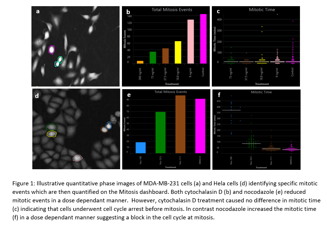
1.         Liu, C.; Neale, Z. G.; Cao, G., Understanding electrochemical potentials of cathode materials in rechargeable batteries. Materials Today 2016, 19 (2), 109-123.

2.         Lain; Brandon; Kendrick, Design Strategies for High Power vs. High Energy Lithium Ion Cells. Batteries 2019, 5 (4).

3.         Yue, Y.; Liang, H., Micro- and Nano-Structured Vanadium Pentoxide (V2O5) for Electrodes of Lithium-Ion Batteries. Advanced Energy Materials 2017, 7 (17), 1602545.

4.         N., N.; F., W.; T., L. J.; G., Y., Li-ion battery materials: Present and future. 2015, 18, 252.

5.         Stringer, J., The vanadium-oxygen system—A review. Journal of the Less Common Metals 1965, 8 (1), 1-14.

6.         Kang, Y.-B., Critical evaluation and thermodynamic optimization of the VO–VO2. 5 system. Journal of the European Ceramic Society 2012, 32 (12), 3187-3198.

7.         Wang, L.; Huang, K. W.; Chen, J.; Zheng, J., Ultralong cycle stability of aqueous zinc-ion batteries with zinc vanadium oxide cathodes. Sci Adv 2019, 5 (10), eaax4279.

8.         Gu, S.; Wang, H.; Wu, C.; Bai, Y.; Li, H.; Wu, F., Confirming reversible Al 3+ storage mechanism through intercalation of Al 3+ into V 2 O 5 nanowires in a rechargeable aluminum battery. Energy Storage Materials 2017, 6, 9-17.

9.         Yoo, H. D.; Jokisaari, J. R.; Yu, Y.-S.; Kwon, B. J.; Hu, L.; Kim, S.; Han, S.-D.; Lopez, M.; Lapidus, S. H.; Nolis, G. M.; Ingram, B. J.; Bolotin, I.; Ahmed, S.; Klie, R. F.; Vaughey, J. T.; Fister, T. T.; Cabana, J., Intercalation of Magnesium into a Layered Vanadium Oxide with High Capacity. ACS Energy Letters 2019, 4 (7), 1528-1534.

10.       Delmas, C.; Brethes, S.; Menetrier, M., ω-LixV2O5—a new electrode material for rechargeable lithium batteries. Journal of power sources 1991, 34 (2), 113-118.

11.       Cocciantelli, J.; Menetrier, M.; Delmas, C.; Doumerc, J.; Pouchard, M.; Broussely, M.; Labat, J., On the δ→ γ irreversible transformation in Li//V2O5 secondary batteries. Solid State Ionics 1995, 78 (1-2), 143-150.

12.       Sides, C. R.; Martin, C. R., Nanostructured Electrodes and the Low‐Temperature Performance of Li‐Ion Batteries. Advanced Materials 2005, 17 (1), 125-128.

13.       Chan, C. K.; Peng, H.; Twesten, R. D.; Jarausch, K.; Zhang, X. F.; Cui, Y., Fast, completely reversible Li insertion in vanadium pentoxide nanoribbons. Nano letters 2007, 7 (2), 490-495.

14.       De Jesus, L. R.; Horrocks, G. A.; Liang, Y.; Parija, A.; Jaye, C.; Wangoh, L.; Wang, J.; Fischer, D. A.; Piper, L. F.; Prendergast, D., Mapping polaronic states and lithiation gradients in individual V 2 O 5 nanowires. Nature communications 2016, 7 (1), 1-9.

15.       Lee, J.-K.; Kim, G.-P.; Song, I. K.; Baeck, S.-H., Electrodeposition of mesoporous V2O5 with enhanced lithium-ion intercalation property. Electrochemistry communications 2009, 11 (8), 1571-1574.

16.       Huo, D.; Contreras, A.; Laïk, B.; Bonnet, P.; Guérin, K.; Muller-Bouvet, D.; Cenac-Morthe, C.; Baddour-Hadjean, R.; Pereira-Ramos, J.-P., Evidence for a nanosize effect on the structural and high performance electrochemical properties of V2O5 obtained via fluorine chemistry. Electrochimica Acta 2017, 245, 350-360.

17.       Pu, J.; Shen, Z.; Zhong, C.; Zhou, Q.; Liu, J.; Zhu, J.; Zhang, H., Electrodeposition Technologies for Li‐Based Batteries: New Frontiers of Energy Storage. Advanced Materials 2019, 1903808.

18.       Meulenkamp, E. A.; van Klinken, W.; Schlatmann, A. R., In-situ X-ray diffraction of Li intercalation in sol–gel V2O5 films. Solid State Ionics 1999, 126 (3), 235-244.

19.       Zhong, W.; Huang, J.; Liang, S.; Liu, J.; Li, Y.; Cai, G.; Jiang, Y.; Liu, J., New Prelithiated V2O5 Superstructure for Lithium-Ion Batteries with Long Cycle Life and High Power. ACS Energy Letters 2019, 5 (1), 31-38.

20.       Liu, H.; Zhu, Z.; Yan, Q.; Yu, S.; He, X.; Chen, Y.; Zhang, R.; Ma, L.; Liu, T.; Li, M.; Lin, R.; Chen, Y.; Li, Y.; Xing, X.; Choi, Y.; Gao, L.; Cho, H. S.; An, K.; Feng, J.; Kostecki, R.; Amine, K.; Wu, T.; Lu, J.; Xin, H. L.; Ong, S. P.; Liu, P., A disordered rock salt anode for fast-charging lithium-ion batteries. Nature 2020, 585 (7823), 63-67.

21.       Lu, Y.; Zhou, X., Synthesis and characterization of nanorod-structured vanadium oxides. Thin Solid Films 2018, 660, 180-185.

22.       Lee, Y., The Effect of Active Material, Conductive Additives, and Binder in a Cathode Composite Electrode on Battery Performance. Energies 2019, 12 (4).

23.       Delmas, C.; Cognac-Auradou, H.; Cocciantelli, J. M.; Ménétrier, M.; Doumerc, J. P., The LixV2O5 system: An overview of the structure modifications induced by the lithium intercalation. Solid State Ionics 1994, 69 (3), 257-264.

24.       Galy, J., Vanadium pentoxide and vanadium oxide bronzes—Structural chemistry of single (S) and double (D) layer MxV2O5 phases. Journal of Solid State Chemistry 1992, 100 (2), 229-245.

25.       Marley, P. M.; Horrocks, G. A.; Pelcher, K. E.; Banerjee, S., Transformers: the changing phases of low-dimensional vanadium oxide bronzes. Chemical Communications 2015, 51 (25), 5181-5198.

26.       Christensen, C. K.; Sørensen, D. R.; Hvam, J.; Ravnsbæk, D. B., Structural Evolution of Disordered Li x V2O5 Bronzes in V2O5 Cathodes for Li-Ion Batteries. Chemistry of Materials 2018, 31 (2), 512-520.

27.       Delmas, C.; Brèthes, S.; Ménétrier, M., ω-LixV2O5 — a new electrode material for rechargeable lithium batteries. Journal of Power Sources 1991, 34 (2), 113-118.

28.       Zhu, J.; Shen, H.; Shi, X.; Yang, F.; Hu, X.; Zhou, W.; Yang, H.; Gu, M., Revealing the Chemical and Structural Evolution of V2O5 Nanoribbons in Lithium-Ion Batteries Using in Situ Transmission Electron Microscopy. Analytical chemistry 2019, 91 (17), 11055-11062.

29.       Mukherjee, A.; Sa, N.; Phillips, P. J.; Burrell, A.; Vaughey, J.; Klie, R. F., Direct Investigation of Mg Intercalation into the Orthorhombic V2O5 Cathode Using Atomic-Resolution Transmission Electron Microscopy. Chemistry of Materials 2017, 29 (5), 2218-2226.

30.       Mukherjee, A.; Ardakani, H. A.; Yi, T.; Cabana, J.; Shahbazian-Yassar, R.; Klie, R. F., Direct characterization of the Li intercalation mechanism into α-V2O5 nanowires using in-situ transmission electron microscopy. Applied Physics Letters 2017, 110 (21), 213903.

31.       Mukherjee, A.; Asayesh Ardakani, H.; Phillips, P. J.; Yassar, R. S.; Klie, R. F., Investigation of Li ion and Multivalent Battery Systems Using In situ TEM and High Resolution EELS. Microscopy and Microanalysis 2015, 21(S3), 1819-1820.

32.       Hussein, H. E. M.; Maurer, R. J.; Amari, H.; Peters, J. J. P.; Meng, L.; Beanland, R.; Newton, M. E.; Macpherson, J. V., Tracking Metal Electrodeposition Dynamics from Nucleation and Growth of a Single Atom to a Crystalline Nanoparticle. ACS Nano 2018, 12 (7), 7388-7396.

33.       Lim, J.; Li, Y.; Alsem, D. H.; So, H.; Lee, S. C.; Bai, P.; Cogswell, D. A.; Liu, X.; Jin, N.; Yu, Y. S.; Salmon, N. J.; Shapiro, D. A.; Bazant, M. Z.; Tyliszczak, T.; Chueh, W. C., Origin and hysteresis of lithium compositional spatiodynamics within battery primary particles. Science 2016, 353 (6299), 566-71.

34.       Macpherson, J. V., A Practical Guide to Using Boron Doped Diamond in Electrochemical Research. Physical Chemistry Chemical Physics 2015, 17 (5), 2935-2949.

35.       Hussein, H. E. M.; Amari, H.; Macpherson, J. V., Electrochemical Synthesis of Nanoporous Platinum Nanoparticles Using Laser Pulse Heating: Application to Methanol Oxidation. ACS Catalysis 2017, 7 (10), 7388-7398.

36.       Hussein, H. E. M.; Ray, A. D.; Macpherson, J. V., Switching on palladium catalyst electrochemical removal from a palladium acetate–acetonitrile system via trace water addition. Green Chemistry 2019, 21 (17), 4662-4672.

37.       Hussein, H. E. M.; Amari, H.; Breeze, B. G.; Beanland, R.; Macpherson, J. V., Controlling palladium morphology in electrodeposition from nanoparticles to dendrites via the use of mixed solvents. Nanoscale 2020, 12(42), 21757-21769.

38.       Armstrong, E.; O'Sullivan, M.; O'Connell, J.; Holmes, J. D.; O'Dwyer, C., 3D Vanadium Oxide Inverse Opal Growth by Electrodeposition. Journal of The Electrochemical Society 2015, 162 (14), D605-D612.

39.       Armstrong, E.; McNulty, D.; Geaney, H.; O'Dwyer, C., Electrodeposited Structurally Stable V2O5 Inverse Opal Networks as High Performance Thin Film Lithium Batteries. ACS Appl Mater Interfaces 2015, 7 (48), 27006-15.

40.       Potiron, E.; Le Gal La Salle, A.; Verbaere, A.; Piffard, Y.; Guyomard, D., Electrochemically synthesized vanadium oxides as lithium insertion hosts. Electrochimica Acta 1999, 45 (1-2), 197-214.

41.       Potiron, E.; Le Gal La Salle, A.; Sarciaux, S.; Piffard, Y.; Guyomard, D., e-V2O5: Relationships between synthesis conditions, material characteristics and lithium intercalation behavior. Journal of Power Sources 1999, 81-82, 666-669.

42.       Li, J. M.; Chang, K. H.; Hu, C. C., The key factor determining the anodic deposition of vanadium oxides. Electrochimica Acta 2010, 55 (28), 8600-8605.


17:27 - 17:28

222 Structured illumination microscopy vs image scanning microscopy

James Manton, Jérôme Boulanger, Nicholas Barry
MRC Laboratory of Molecular Biology, Cambridge, United Kingdom

Abstract Text

Both structured illumination microscopy (SIM) and image scanning microscopy (ISM) can surpass the usual wide-field fluorescence diffraction limit by a factor of two, but achieve this performance through different means and image processing routines. Hence, it is often not clear which method is superior in a given situation, nor indeed whether this question has a definite answer.

First, we introduce a fast reconstruction routine that can process both SIM and ISM data, in real-space. We show how this can be applied to any illumination pattern, including fringes, spots, lattices and lines. Next, we use numerical simulations to compare the performance of SIM and ISM at depth, where background signal and refractive index mismatch degrade the performance of both techniques. Finally, we attempt to compare the relative phototoxicities of each technique, using photobleaching as a substitute metric.

Using these results, we provide guidelines for the selection of an appropriate technique and an outlook on future developments that may enhance performance further still.

Keywords

structured illumination microscopy, image scanning microscopy, super-resolution, extended-resolution, image formation, image processing, deconvolution


17:28 - 17:29

224 Automated In-Situ Spectrum Imaging with Synchronized Stimulus Control

Dr Liam Spillane, Dr Benjamin Miller, Dr Bernhard Schaffer, Dr Paul Thomas, Dr Ray Twesten
Gatan Inc., Pleasanton, USA

Abstract Text

The scanning transmission electron microscope (STEM) is a well-established analytical tool for characterizing material structure-property relationships due to the large number of signals result from the beam-specimen interaction, combined with the fact that many can be acquired simultaneously at high spatial resolution. 

Spectrum imaging (SI), a modality enabling the acquisition of spatially resolved analytical signals, is particular powerful due its capability to enable direct correlation between imaging and analytical data. Three primary types of STEM-SI have been widely adopted. Diffraction spectrum imaging (4DSTEM, CBED-SI) gives morphological and crystallographic information. Energy dispersive (x-ray) spectroscopy (EDS) SI, and electron energy-loss spectroscopy (EELS) SI give compositional information. EELS can also be used to probe local electronic structure, allowing local determination of: bonding states, chemistry, phonon and/or electronic band structure. For in-situ STEM-SI analysis, multiple SI passes must be acquired, making the ability to record data at high speed and high dose efficiency particularly important [1]. In order to avoid missing important transformations during an experiment, high in-situ stimulus resolution is also of fundamental importantance [1].

In this work, we use a CMOS based transmission electron counting detector fitted into an optimized post-column energy filter (K3 Continuum-IS) to demonstrate recent advances in synchronized in-situ spectrum imaging acquisition. These advances allow fully automated acquisition of the CBED and EDS signals at a given in-situ condition, in addition to the EELS signal, maximizing the information that can be extracted from a single specimen and target region of interest Additionally, datasets are now streamed/written directly to disk rather than held memory in over the duration of the experiment, following the workflow steps shown in figure 1. The combined effect of these advances maximizes the information that can be extracted from a single specimen, even for irreversible transformations as all data can be acquired in a single experiment, in addition to maximizing the stimulus resolution at which the data can be captured.

Metal oxide systems have been used as model materials systems. Example dual-EELSTM, energy-filtered diffraction and EDS multipass spectrum image results acquired from silver (II) oxide over temperature range 25 – 600°C are shown in figure 2. Temperature control was implemented as per the flow diagram show in figure 1. In this presentation we will expand upon these findings to highlight the importance and impact of automation and synchronization to in-situ STEM analysis.


Uncaptioned visual

Figure 1. Flow diagram showing data acquisition and holder control steps in the multimodal multiple pass spectrum imaging method.


Uncaptioned visual

Figure 2. Multimodal SI data acquired from silver(II) oxide powder at 600°C: (a) energy filtered CBED pattern showing virtual aperture positions for (b) orientation map. (c) EELS Ag M-edge map, and (d) EDS Ag L-peak map. Equivalent data for 25°C is also shown (e-h).  


Keywords

STEM, EELS, EDS, CBED, 4DSTEM, in-situ, heating, automation, multimodal, DMScript, Python, Scanning Transmission Electron Microscopy, Electron Energy-Loss Spectroscopy, Diffraction, Convergent Beam Electron Diffraction, Catalysis, Metal Oxide, Electron Counting, Counting EELS, 

References

[1] L. Spillane et al., Microsc. Microanal. 26 (Suppl 2), (2020)


17:29 - 17:30

227 Eliminating charging issues when imaging non-conducting physical and biological samples by FIB tomography

Xiangli Zhong, James O'Sullivan, Philip J Withers
The University of Manchester, Manchester, United Kingdom

Abstract Text

This work serves as a guideline and provides theoretical explanation for charging elimination for focused ion beam (FIB) tomography of nonconductive physical and biological samples.

FIB damage can lead to unreliable imaging and lead to artifacts and incorrect interpretations (Zhong et al.). Eliminating FIB damage to physical and biological samples is one of the most important aspects for 2D and 3D FIB analysis.  Here we report on experimental procedures and the theoretical aspects relating to charging of non-conducting samples. A polymeric paint sample and a biological tissue sample are considered in this study by way of exemplars.

We found that ion beam milling of resin epoxy can lead to the milled face change from non-conducting nature to conducting. Fig. 1 shows the results of FIB serial sectioning volume microscopy of a polymeric paint sample which was coated with 30nm Au pre-coating.  An exemplar slice in Fig.1a shows the epoxy matrix of the paint sample has become electronically conductive. However, the surfaces of the silica pigments are still non-conducting. The FIB modification (or ‘FIB healing’) of the epoxy could be due to the hydrogen-carbon bond of the hydrocarbon molecule chain breaking and the H evaporating into the vacuum chamber of the FIB system during the high energy ion beam bombardment.   Fig. 2a is the schematic representation of the epoxy under ion beam where H disappeared leaving with conjugated benzene and C where the flow of electrons is enhanced. Our initial Raman test indicates the chemical degradation and structural modification may eventually lead to a predominantly carbon containing film, thus the milled face exhibits good electronic transport properties(De Bonis et al.).  

A tissue block prepared by a biological SEM sample preparation protocol of fixation, staining, dehydration and embedding was used here as an example. Fig. 3a shows the blistering on the sample surface caused by insufficient coating. Fig. 3b shows improved imaging upon coating to sufficient thickness. No charging issue was found throughout the 400 slices of the 3D volume thanks to the ‘ion beam healing’ effect where ion beam modified slice faces could be imaged well using electron beam without charging issue. No damage was found on any of the slices.

Gold or other metal sputter coating is commonly used to minimise charging for scanning electron microscopy (SEM). The typical coating thickness is in the range of 3-10 nm. However, it is not sufficient to eliminate the sample charging issue for FIB 2D cross-sectional or 3D serial imaging analysis.   More than 30nm of Au pre-coating is required for FIB 2D cross-sectional analysis as shown in Fig 2b. The experimental results agrees well with the SRIM (Stopping and Range of Ions in Matter) simulation of the ion recoil range(Ziegler et al.).  In consideration of sputtering of the pre-coating during 2D or 3D FIB analysis, sufficient pre-coating is a crucial factor to enable a reliable FIB experiment. For serial sectioning 3D FIB analysis, the in-situ protective coating (usually Pt) thickness required depends on the number of slices and slice thickness. In general, the bigger the 3D volume to be analysed, the thicker the protective coating needs to be. This is due to the progressive sputtering of the protective coating during 3D volume acquisition.   

In conclusion, the ion beam modification of the milled face acts as a ‘healing power’ for the nonconductive epoxy resin faces which enables the slice face become electron conductive.       Thicker pre-coating than conventional SEM sample surface treatment is required. More than 30nm of Au pre-coating is suggested. Protective Pt coating thickness needs to be consistent to the number of slices and the volume of the 3D serial sectioning. 

Uncaptioned visual Uncaptioned visual

                       (a)                                                        (b)

Fig. 1 FIB volume microscope analysis of a polymeric paint sample with non-conducting pigments, a) FIB slice showing the elimination of charging on epoxy resin whilst charging of the non-conducting pigments SiO2 is evident b) 3D volume representation of the FIB serial sectioning tomography. 


Uncaptioned visual Uncaptioned visual

            (a)                                                  (b)


Fig. 2 Mechanism of the charging elimination. a) Debonding and evaporation of H during ion beam bombardment resulting in conjugated structure. b) SRIM simulation indicated the ion recoil distribution at 30nm thickness where limited ions has recoiled into the non-conducting sample.


Uncaptioned visual Uncaptioned visual

                                (a)                                                                     (b)


Uncaptioned visual


Fig. 3 3D block surface of the resin block embedded with biological tissue. a) 10nm Au pre-coating. b) 40nm Au pre-coating.  c) Tissue cellular structure observed without charging or damage during serial FIB cross-sectional milling, representation slices showing the slice number 50th, 100th, 200th and 400th.

Keywords

FIB, Damage, Charging, Polymer, Biological samples, FIB tomography, Coating, 3D, conductive, SEM

References

De Bonis, A., et al. “Structural Modifications and Electrical Properties in Ion-Irradiated Polyimide.” Nuclear Instruments and Methods in Physics Research, Section B: Beam Interactions with Materials and Atoms, vol. 151, no. 1–4, 1999, pp. 101–08, doi:10.1016/S0168-583X(99)00135-4.

Zhong, Xiangli, et al. “Comparing Xe+pFIB and Ga+FIB for TEM Sample Preparation of Al Alloys: Minimising FIB-Induced Artefacts.” Journal of Microscopy, no. July, 2020, pp. 1–12, doi:10.1111/jmi.12983.

Ziegler, James F., et al. “Nuclear Instruments and Methods in Physics Research B SRIM – The Stopping and Range of Ions in Matter ( 2010 ).” Nuclear Inst. and Methods in Physics Research, B, vol. 268, no. 11–12, Elsevier B.V., 2010, pp. 1818–23, doi:10.1016/j.nimb.2010.02.091.


17:30 - 17:31

230 Inverted microscope platform for cryo-CLEM and laser-free confocal cryo-fluorescence

Michael Schwertner1, Phillipa Timmins2, Kirti Prakash3, Stephanie Rey3, Mike Shaw3
1Linkam Scientific Instruments Ltd., Tadworth, United Kingdom. 2Aurox Ltd., Abingdon, United Kingdom. 3National Physical Laboratory, Teddington, United Kingdom

Abstract Text

Cryo-imaging of biological samples embedded in vitrified ice has unique advantages and the development and implementation of cryo-EM and single particle analysis led to a Nobel Prize in 2017 [1]. More recently cryo-EM was also used for research into the structure and mechanisms of the coronavirus [2].

Fluorescence cryo-imaging in confocal and widefield modes can support the electron microscopy workflow in several ways. Firstly, in the form of CLEM (Correlative Light and Electron Microscopy), where fluorescence imaging of samples allows the use of specific and sensitive markers not available in EM. CLEM also limits sample EM beam damage through pre-identification of ROI’s in a light microscope (LM) image with subsequent matching of coordinates. Secondly, cryo-imaging in the LM allows sample pre-screening and assessment of preparation quality saving costly EM time.

Current cryo-stage designs for fluorescence are typically for upright microscope setups and cannot be integrated with the inverted widefield or confocal fluorescence systems commonly found in bio-labs. While inverted-upright conversion optics are available [3], typical implementations do not allow straightforward sample loading. Here we describe a prototype for the integration of a CMS196V3 (upright) cryo-stage into an inverted microscope system (Nikon Eclipse Ti-E with Aurox Clarity Laser-Free Confocal) with a tilt mechanism for the direct loading of cryo-samples. In this talk we will discuss the hardware integration of the cryo-stage and the Clarity system (see figures 1,2,3), the software integration based on MicroManager (Fiji) [4] and share PSF measurements to assess the optical performance of the conversion system.

Uncaptioned visual

Figure 1: Overview of the system on Nikon Ti platform with Linkam CMS196 cryo-stage and Aurox Clarity laser-free confocal unit.


Uncaptioned visual

Figure 2: Linkam cryo-stage with engaged tilt-arm.


Uncaptioned visual

Figure 3: Optical arm tilted back for sample loading and manipulation.

We anticipate that the convenience of sample loading combined with integration into more common microscope systems and the flexible software architecture can lead to a wider adaptation of cryo-fluorescence and CLEM.

First cryo-confocal images were imaged with the system on HeLa cells marked with GFP and plunge-frozen at NPL on R2/2 gold grids (Quantifoil).

Figure 4 shows a low-magnification cryo-confocal overview (maximum intensity projection) of a sparsely populated grid while figure 5 shows a single cell from the same sample imaged with the 100x NA 0.9 lens under cryo-conditions.


Uncaptioned visual

Figure 4: 10x cryo-confocal overview image, HeLa Cells.


Uncaptioned visual

Figure 5: Cryo-Confocal image (maximum intensity projection of stack) of HeLa cell with GFP staining using 100x NA 0.9 WD=2.0 mm objective lens and LED illumination (466 nm) coupled to Clarity laser-free confocal unit.


Keywords

cryo-fluorescence (cryo-FM), cryo-EM, cryo-ET, cryo-CLEM (Correlative Light and Electron Microscopy), cryo-TEM, inverted-upright conversion relay optics

References


17:32 - 17:33

234 Speckle based Phase Contrast X-ray Microscopy, an investigation into possible clinical and research applications.

Mr Matthew Donoghue1, Dr Hongchang Wang2, Dr. Daniel O'Toole3, Dr. Charles Connolly1, Dr Sean Hynes4, Ms Terri Muldoon4, Mrs Brid King1, Dr Shad Horie3, Dr Christoph Kleefled3, Mr Brendan Tuohy4, Dr Peter Woulfe1
1Galway Clinic, Galway, Ireland. 2Diamond Light Source, Harwell, United Kingdom. 3National University of Ireland Galway, Galway, Ireland. 4University Hospital Galway, Galway, Ireland

Abstract Text

This study aims to assess and advance the potential of Speckle based Phase Contrast X-ray Microscopy for clinical diagnosis of various pathologies. A collaborative group between Galway Clinic, University Hospital Galway (UHG), National University of Ireland Galway (NUIG), and Diamond Synchrotron Facility, UK, has been set up to investigate the potential of this imaging technique. The aim of this group is to develop a clinically implementable x-ray microscopy system that will allow micron scale imaging over a gross tissue volume; allowing for morphological analysis of soft tissue microstructures (e.g. micro vascularisation) and  cellular structures (e.g. cell nucleus) in one tomographic scan. 


Phase contrast Imaging (PCI) is a technique that may offer a solution to the limitation of conventional x-ray microscopy systems. PCI comprises a range of new techniques that rely on phase shifts induced by a sample to produce an image, rather than absorption differentials for current clinical imaging methods.(1)  One such technique created by members of the research group at Diamond is referred to as 1D Speckle based phase contrast imaging. Speckle based PCI measures phase shifts by initially taking a reference image of a diffuser. This is composed of “speckles” generated by the grains of sand, A second image, the sample image, is then taken with a sample upstream of the diffuser. The digital image analysis software is used to compare between the two images and track the displacement of the speckles induced by the sample, therefore the phase shift of the x-ray photons as they transverse through the sample can be reconstructed. This results in a soft tissue image signal at certain photon energies in the range of two to three orders of magnitude larger than a standard absorption signal. (2,3)


Methodology 

A number of various tissue samples were imaged, these included human breast, human kidney, rat brain and two rat lung samples one pneumonia and one control. Patient consent  and ethics approval from the local ethics committees were given.  All samples were fixed with formaldehyde and embedded in a paraffin wax before transport to Diamond Light Source. Once there a number of 1mm dimeter cores were taken in preparation for the scan.     

During these studies a polychromatic beam of x-rays with a mean energy of 15 KeV was used. This was achieved through the filtering of the broadband beam through 2mm sheet of Copper. Abrasive paper with an average particle size of 5µm was mounted on a motorised stage located 47 m from the x-ray source.

Tissue samples of size of ~1mm diameter will be placed on a motorised linear translation stage 0.2m upstream of the abrasive paper. The detector should be placed placed ~1m upstream from the sample, this was done to maximise angular sensitivity using this beamline. In previous experiments x-ray detector comprised of a mirror backed LuAG scintillator, variable objective microscopic lens and a PCO edge camera. This allowed an effective pixel size of 1.1µm for the 1mm sample diameter arrangement, in this experiment we hope to alter the detector setup to achieve 0.75µm effective pixel size.

In the previous experiment a series of images were taken as the abrasive paper translated horizontally across the sample in 30 sub pixel step sizes. Subsequently, absorption, dark-field, horizontal and vertical phase images were extracted with pixel-wise analysis using a cross-correlation algorithm for each diffuser position. The phase contrast image was then reconstructed by partial integration of the two orthogonal differential phase contrast images. The sample will be mounted on a high-speed rotation stage, and the recent developed fly-scan X-ray phase tomography will be carried out. (4) This can be repeated in the purposed experiment. 

Results

The images produced from the scan were compared to H&E stained slices imaged at 20 magnification from the same 1mm cores. A high degree of similarity was noted although it was not possible to conclusively identify cell type by the phase scan alone. Due to the 3-D volumetric nature of the phase scan information regarding variation in gross tissue structure could be easily retrieved. For example this was used to measure the degree of inflammation of alveolar tissue through a quantitative metric which may be beneficial in the study of inflammatory lung diseases such as COPD.       

Conclusion

The Speckle based Phase Contrast technique was successful in produced images of high soft tissue signal to noise ratio when compared to the equivalent absorption images. Individual cells were discernible although it was not possible to conclusively identify the cells through the phase contrast images alone. Further work is ongoing to identify cells through alternative means such as radiomic analysis of identified cells through cross comparison with immunostained microscopy slides. 


Keywords

X-ray phase contrast, tomography, histology 

References

1] Interface-specific x-ray phase retrieval tomography of complex biological organs (2011), M Beltran, D Paganin, K Siu, Phys. Med. Biol. 56 7353

2] X-ray phase contrast tomography by tracking near field speckle (2014), H Wang, S Berujon, J Herzen, D Lundy, Nature Scientific Reports, 5:8762

3] From Synchrotron radiation to lab source: advanced speckle-based X-ray imaging abrasive paper (2015), H Wang, Y Kashyap, K Sawhey, Nature Scientific Reports, 6:20476


4] High-energy, high-resolution, fly-scan X-ray phase tomography. (2019) Wang, H. R. Atwood, M Pankurst. Sci. Rep. Nature Scientific Reports 9: 8913


17:33 - 17:34

236 Probing the structure-property relationship in natural and bioinspired dental materials aided by in situ advanced microscopy

Dr Tan Sui
University of Surrey, Guildford, United Kingdom

Abstract Text

Dental caries is one of the most prevalent, yet preventable, chronic diseases that heavily impacts the aesthetics and function of teeth and can cause oral pain. Therefore, there has been a growing demand for restorative products (e.g. dental crowns) with significantly improved service life and mechanical performance to replace the lost teeth due to this disease. This research is devoted to the long-term goal of improving the dental care of patients with a two pronged approaches. The first is to use advanced synchrotron X-ray techniques: small- and wide- angle X-ray scattering (SAXS and WAXS) and tomography to expand the knowledge of the structural evolutions that occur in dentine and enamel, subjected to caries-causing environment such as acid demineralisation. This will aid the development of therapeutic treatments designed to regain the structural integrity of carious dental tissues. The second is to use advanced mechanical microscopy techniques that include in situ scanning electron microscopy (SEM) mechanical testing, in situ nanoindentation and Plasma Focused-ion-beam and digital-image-correlation (PFIB-DIC) to study the micromechanics of bi-directional freeze-casted novel bioinspired dental materials, e.g. ceramic-polymer composites. This will aid the microstructure design and optimisation with significantly improved resilience to fracture as well as the development of novel bioinspired tough and cost-effective ceramic-based composite materials as the next generation dental crown materials.

Keywords

dental caries, bioinspired ceramic-based composite, synchrotron X-ray techniques, in situ SEM analysis, in situ nanoindentation, PFIB-DIC

References

  1. T Sui, et al. In situ monitoring and analysis of enamel demineralisation using synchrotron X-ray scattering, Acta Biomater., 77 (2018).
  2. H Wan, N Leung, S Algharaibeh, T Sui, Q Liu, H Peng, B Su, Cost-effective fabrication of bio-inspired nacre-like composite materials with high strength and toughness Composites Part B: Engineering, 202, 108414 (2020).

17:35 - 17:36

272 Routine Sample Optimization for Single Particle Cryo-EM with chameleon

Development Scientist Michele Darrow, Product Manager Paul Thaw, Busineess Development Manager Tim Booth
SPT Labtech LTD, Melbourn, United Kingdom

Abstract Text

The period responsible for the current generation of cryogenic electron microscopy (cryo-EM) instruments and image processing software is often referred to as the “resolution revolution.” The results of these technological advancements have been achievements in higher quality structures and cryo-EM becoming the go-to method for structural biologists. However, sample preparation is widely recognized as a key unresolved step in the high resolution cryo-EM workflow. [1]

With the introduction of next generation sample preparation methods realized through emerging instruments such as chameleon, researchers can drive optimization towards repeatable high-resolution outcomes on a single platform. The chameleon is routinely used to empirically determine the sample dependent behavior for a given concentration, buffer condition and ice thickness for a range of dispense-to-plunge times. With this information subsequent steps can be directed using optimal conditions to mitigate negative effects unique to the biological sample at hand.

The literature demonstrates the clear benefits of chameleon as a platform for obtaining specimen with improved quality using traceable outcome driven decision making. Incorporating the chameleon into the cryoEM workflow and enabling discrete dispense-to-plunge time characterization for the sample at hand represents a paradigm shift in the approach to sample optimization bottlenecks and reduces the knock-on costs (time and money) caused by poor sample quality downstream.

Protein adsorption to the air-water interface during the thin film formation step represents the main obstacle bottlenecking the workflow towards routine structure determination of single particles by high resolution cryo-EM. This behavior can be described by a three-step process. First the diffusion mediated initial adsorption of the protein at the interface, followed by denaturation or unfolding of the adsorbed protein and finally the formation of a ‘film’ with chemical and mechanical properties related to the rate of adsorption and protein stability in solution. [2,3]

We now know air-water interface effects are ubiquitous [5] but due to a large variety of contributing factors, the effects of the denatured film are likely non-uniform. [6,7] The process scales roughly with protein concentration [4] and a combination of specific molecular characteristics influences the rate of adsorption at the interface. [7]

A common effect of conventional slow (> 1 sec) blotting or pin printing techniques is up to a 30-fold increase in sample concentration at the air-water-interface. [8] The denaturation and unfolding, which is pronounced for less stable proteins, leads to low sample quality and results in limited achievable resolutions and the need to collect large data sets with a very low percentage of particles remaining in the resulting reconstructions.

Advancements in automation and self-wicking grid technology allow for controlled and predictable thin film formation resulting in targeted ice thickness at discrete fast plunge times up to 54ms. chameleon has been shown to reproducibly obtain improvements in sample quality using plunge times an order of magnitude faster than the times available using commercially available conventional blotting or pin printing technology. Self-wicking grids are optimized for sample specific thin film formation and are dependent on concentration and viscosity.

Recent data suggests that for a given sample and concentration, faster plunge times lead to a reduction in the concentrating effect at the air water interface and therefore, lower observed particle density correlated to faster plunge times. Although the relationships are non-linear and sample dependent, early use suggests an understanding of this effect for each, and every sample is critical to determining an optimization pathway towards improved sample quality for high resolution.

Rather than eliminate all interactions between protein and the air water interface, since it is impractical to outrun protein adsorption entirely, routine chameleon protocols target a range of discrete dispense-to-plunge times to initially characterize sample behavior with regards to concentration, wicking speed, film thickness and observable particle density and then optimize based on outcomes.

Approaching the chameleon with a new sample requires a first step to determine the fastest plunge time possible for a given sample concentration without particle density dropping too low. Using the sample concentration in hand or 2x when available, the system is directed to prepare a few grids at a range of reducing plunge times. Typically, the plunge time range will start at > 500ms for observable particle densities comparable to conventional methods. The starting plunge time of 500ms, slow by chameleon standards, represents a 2-10x reduction in dwell time compared to other commercially available sample preparation instruments. Grids are accepted at a range of ice thickness from ‘good’ to ‘overwicked.’ Early results point to improvements in specimen quality across a variety of samples for a range of sample-specific plunge times.

After gaining an understanding of the appropriate plunge time range and ice thickness for the sample concentration and characteristics, a second freezing session with a set of much more stringent acceptance criteria corresponding to a smaller range of plunge times and film thickness can produce multiple examples with consistent outcomes.

The conventional or traditional sample preparation methods for cryo-EM result in extreme, sample dependent differences between specimen prepared in a similar manner and due to this a variety of experimental methods have been developed over the last 40 years to deal with the subsequent detrimental behavior. Each method requires its own optimization routine, possibly utilizing multiple instruments.

There are not yet any optimization workflows specific to sample type. Only a consensus that optimization is required for most samples and that approximately ten different methods will be attempted in combination before improvement is seen. Additionally, none of the currently available methods can be determined to work in advance of sample preparation. [1]

The routine optimization protocol available through chameleon represents a paradigm shift by addressing the unique sample dependent air-water interface effects by adjusting the vitrification step to the sample behavior instead of requiring researchers to introduce additional methods to modify sample behavior to accommodate standardized plunge freezing devices.

To be able to capture biochemistry consistently and confidently researchers need the ability to freeze where and when the biochemistry is carried out, placing the requirement for change squarely on the sample preparation devices to modernize, improve ease-of-use, and generate outcomes efficiently to achieve early milestones routinely.  


Keywords

cryoEM, sample preparation, sample optimization, air water interface, inkjet dispensing, nanowire grids, self-wicking, plunge time control, chameleon, thin film formation, ice thickness

References

  1. B. Carragher, Y. Cheng, A. Frost, R.M. Glaeser, G.C. Lander, E. Nogales, H.-W. Wang, Current outcomes when optimizing ‘standard’ sample preparation for single-particle cryo-EM doi:10.1111/jmi.12834 Published: September 19, 2019
  2. Razumovsky L, Damodaran S. Surface Activity−Compressibility Relationship of Proteins at the Air−Water Interface. Langmuir. American Chemical Society; 1999 Feb;15(4):1392–9. 
  3. Martin AH, Grolle K, Bos MA, Cohen Stuart MA, van Vliet T. Network forming properties of various proteins adsorbed at the air/water interface in relation to foam stability. J Colloid Interface Sci. 2002 Oct 1;254(1):175–83. 
  4. Israelachvili, JN (2011) Intermolecular and Surface Forces, 3rd edn, Elsevier, Amsterdam: Academic Press.
  5. A Noble, et al. Nature Methods 15 (2018), p. 793-795.
  6. Gunning PA, Mackie AR, Gunning AP, Woodward NC, Wilde PJ, Morris VJ. Effect of Surfactant Type on Surfactant−Protein Interactions at the Air−Water Interface. Biomacromolecules. American Chemical Society; 2004 May;5(3):984–91. 
  7. De Jongh HHJ, Kosters HA, Kudryashova E, Meinders MBJ, Trofimova D, Wierenga PA. Protein adsorption at air-water interfaces: A combination of details. Biopolymers. John Wiley & Sons, Ltd; 2004;74(1-2):131–5. 
  8. Klebl et al., Need for Speed: Examining Protein Behavior during CryoEM Grid Preparation at Different Timescales, 2020, Structure 28, 1238-1248

17:36 - 17:37

273 High energy resolution STEM-EELS as a powerful tool for the characterisation of battery materials

Angelica Laurita1, Jérémie Auvergniot2, Liang Zhu2, Pierre-Etienne Cabelguen2, Dominique Guyomard1, Nicolas Dupré1, Philippe Moreau1
1Université de Nantes, CNRS, Institut des Matériaux Jean Rouxel, IMN, 2 rue de la Houssinière, F-44000 Nantes Cedex 3, France. 2Umicore, Rechargeable Battery Mat, 31 Rue Marais, BE-1000 Brussels, Belgium

Abstract Text

The electrification of vehicles presently relies on lithium ion batteries using layered oxides of nickel, manganese and cobalt (NMC) with high Ni content as positive electrode materials. Nevertheless, it has been demonstrated that these materials suffer from gassing issues decreasing cycle life and causing safety problems. Moreover, nickel-rich NMCs are affected by critical instability during all the manufacturing steps (synthesis, handling, electrode preparation). A deep comprehension of the pristine material properties and of its behaviour during electrode preparation and electrochemical cycling is thus fundamental from the industries’ point of view.

In this context a systematic study of the surface reactivity of NMC811 (Li[Ni0.8Mn0.1Co0.1]O2) was conducted using a multi-analytical approach in which transmission electron microscopy plays an essential role. A new TEM/STEM Themis Z G3 (Thermo Fisher Scientific) equipped with a double camera GIF spectrometer, was recently installed in the Jean Rouxel Institute of Materials of Nantes (France). Electron Energy Loss Spectroscopy (EELS) was in particular exploited in order to give a complete description of the surface of the material.

The direct detection camera (Gatan K2 Summit) allowed the acquisition of EELS spectra in STEM mode with both high energy and spatial resolution. This enables a good multi-elemental chemistry mapping quantification (at low energy dispersions) as well as the accurate analysis of the fine structures of the Ni L23 -edges thanks to the use of an excited monochromator. Moreover, the use of a vacuum transfer sample holder insured the observation of samples without any contact with the ambient atmosphere. The samples were in fact transferred directly to the microscope from the Argon glove box where they were stored, preventing any sort of reaction of the material with air and thus allowing the proper analysis of the material in its initial state.

In this way it was possible to look at the surface modifications and to compare them to the bulk structure by means of both the multiple linear least square (MLLS) fitting and the Principal Components Analysis (PCA); the thickness of the surface modified layer was then determined for all the samples, proving the high reactivity of the material surface in humid atmosphere. The Ni L3-edge changes in fact between the surface and the bulk of the material, indicating its oxidation state’s evolution after 2 days in 30% of Relative Humidity. The reduced Ni was found for about the first 15 nm of the surface. 

On the other hand, the analysis of the same powder transferred directly from the glove box revealed a similar behaviour of the Ni L-edge (Figure 1) in the first 6 nm of surface only; a slight change in the 

Uncaptioned visual

Figure 1: Evolution of Ni L3-edge in the pristine NMC 811 powder


shape of the oxygen K-pre-edge was also observed, indicating that a gradual but not yet completed evolution of the material surface.

Moreover, through the calculation of the second derivative of the EELS spectra, a quantification of all the transition metals was performed. It has to be considered here that the small quantity of Mn and Co in the material doesn’t usually allow the correct quantification of these species, since the corresponding intensity signal is too low and often confused into the background. For this reason, changes in the surface composition of this materials have rarely been deduced by EELS spectra at this level of precision.

Uncaptioned visual

Figure 2: STEM-EELS Zero-Loss Peak intensity on a FIB lamella of a NMC811 secondary particle


In addition to primary particle analysed above, FIB lamellas (Figure 2) were also produced on secondary particles (made of these primary particles) actually used by our industrial partner. First results on these closer to application samples will be presented so that we can demonstrate how the observed phenomena on primary particles translate at a larger scale. 

To conclude, EELS Spectrum Images were analysed in order to obtain qualitative and quantitative information about the surface of NMC811, essential to the good comprehension of its reactivity and gassing behaviour. EELS was used for the determination of both the valence state, coordination and quantity of all the transition metals as well as for the qualitative identification of surface modifications in particular aging conditions.


17:37 - 17:38

276 Quantum on a budget: Developing a 3d-printed microscope for Optically Detected Magnetic Resonance of nanodiamond

Mr Ryan Corbyn1,2, Miss Rebecca Craig1, Miss Gemma Cairns1,3, Dr Brian Patton1
1University of Strathclyde, Glasgow, United Kingdom. 2Diamond Science and Technology CDT, University of Warwick, Coventry, United Kingdom. 33. Optima CDT, University of Edinburgh, Edinburgh, United Kingdom

Abstract Text

Even high-purity diamonds contain crystallographic defects, some of which have been shown to be fluorescent under optical excitation [1]. The Nitrogen-Vacancy (NV) defect, comprised of a substitutional nitrogen beside a vacancy, has seen a lot of interest due to its optical activity, with an emission spectra reaching into the near IR [2]. The extra electron in the negatively charged NV centre (NV-) leads to quantum-mechanical spin effects in the emission that can be exploited for optically detected sensing of magnetic fields and remote thermometry [3].  

After excitation by a green light source, the NV- centre can decay via either the emission of a photon (637-800nm) or via a phonon mediated intersystem crossing event [2]. This dual decay pathway is exploited in Optically Detected Magnetic Resonance (ODMR) experiments: The ground state of the NV- is split into 3 levels by spin state, with the ±1 spin states 30% more likely to decay via the intersystem crossing decay path without the emission of a visible photon [4]. Therefore, if the fluorescence intensity from the defect is monitored while an applied variable frequency microwave field is scanned around the resonant frequency of the NV- centre, the spin-state transition energies can be determined.   

We are particularly interested in the applications of fluorescent nanodiamonds (FNDs), diamond crystals that are between 5-100nm in diameter and contain NV centres upon which we can perform ODMR. Previous work has shown that nanodiamonds are biocompatible [5] and have been successfully integrated into live biological samples to measure local environmental temperature changes within the sample by monitoring the (microwave) resonant frequency of the NV- centre [7 ,8].  

The work cited above used costly, complex microscopes systems to perform these experiments. For the best sensitivity and flexibility, it is likely that many future applications will still need similar systems. However, low-cost alternatives can also offer significant benefits. In this presentation we will outline the progress made so far to develop a 3D printed, lower-cost microscope system capable of performing ODMR measurements on nanodiamonds. We will discuss the parameters that need to be taken into consideration when designing and testing the system, such as: Microscope design, camera quality, sample tracking, sample illumination, the microwave source, and present our latest results from test systems, including our initial estimations of the scope of experiments which are feasible using this system within realistic timescales and budgets.  


Keywords

3D printed microscopes, Optical sensing

References

[1] Jelezko, F. & Wrachtrup, J. Single defect centres in diamond: A review. phys. stat. sol. (a) 203, 3207–3225 (2006). 

[2] Doherty, M. W. et al. The nitrogen-vacancy colour centre in diamond. Physics Reports 528, 1–45 (2013). 

[3] Wojciechowski, A. M. et al. Precision temperature sensing in the presence of magnetic field noise and vice-versa using nitrogen-vacancy centers in diamond. Appl. Phys. Lett. 113, 013502 (2018). 

[4] Rondin, L. et al. Magnetometry with nitrogen-vacancy defects in diamond. Rep. Prog. Phys. 77, 056503 (2014). 

[5] Schrand, A. M. et al. Are Diamond Nanoparticles Cytotoxic? J. Phys. Chem. B 111, 2–7 (2007). 

[6] Kucsko, G. et al. Nanometre-scale thermometry in a living cell. Nature 500, 54–58 (2013). 

[7] Fujiwara, M. et al. Real-time nanodiamond thermometry probing in vivo thermogenic responses. Science Advances 6, (2020). 


17:38 - 17:39

285 Modular, sustainable, low-cost, open microscopy and high content analysis

Mr Jonathan Lightley1, Dr Frederik Görlitz1, Dr Sunil Kumar1,2, Dr Ranjan Kalita1, Mr Arinbjorn Kolbeinsson1, Dr Edwin Garcia1, Dr Yuriy Alexandrov1,2, Mr Simon Johnson1, Mr Martin Kehoe1, Dr Vicky Bousgouni3, Mr Riccardo Wysoczanski1, Mr Dan Marks1, Professor Iain McNeish1, Professor Peter Barnes1, Professor Louise Donelly1, Professor Chris Bakal3, Mr Callum Hollick4, Mr Jeremy Graham4, Professor Christopher Dunsby1,2, Profesor Mark Neil1,2, Dr Seth Flaxman1, Professor Paul French1,2
1Imperial College London, London, United Kingdom. 2Francis Crick Institute, London, United Kingdom. 3Institute of Cancer Research, London, United Kingdom. 4Cairn Research Ltd, Faversham, United Kingdom

Abstract Text

Summary

We present an open source microscopy platform that can be configured for a wide range of microscopy modalities to deliver performance comparable to commercial research microscopes. Here we report an exemplar implementation of super-resolved HCA, demonstrating automated multiwell plate dSTORM implemented with a low-cost multimode diode lasers, a robust optical autofocus module and a new class of low-cost, cooled CMOS camera. These modules can be implemented with the open, modular openFrame microscope stand

Introduction

Fluorescence microscopy has been revolutionized by the development of advanced microscopy techniques including super-resolved imaging, quantitative phase contrast imaging, hyperspectral imaging. While SRM techniques, in particular, have transformed expectations for cell microscopy, commercial SRM instruments can be unaffordable for many researchers. We have been developing a range of self-built microscopes, including STED and dSTORM instruments and automated microscopes for high content analysis (HCA). Having worked to adapt legacy commercial microscope frames to new modalities, we realised that commercial microscope frames already present a significant cost to lower resource settings and proprietary hardware and software can add challenges to such self-build projects. Accordingly, we have developed a new, modular open source microscope frame, “openFrame”, that aims to minimise cost and to simplify the set-up of self-built advanced microscopes while providing research quality performance. Here we present an implementation of automated dSTORM microscopy with optical autofocus and open source software for image data acquisition and analysis. openFrame sits within our openScopes platform that aims to provide cost-effective access to advanced optical imaging techniques including high content analysis, super-resolved microscopy, quantitative phase contrast imaging and hyperspectral imaging. 

Uncaptioned visual

Methods

Figure 1 illustrates the openFrame concept, which is designed around a cylindrical geometry that allows straightforward centering of components along an optical axis and it is made up of different layers that can be customized as necessary for specific applications. It has been designed for straightforward manufacture using standard lathes and milling machines. openFrame has a top layer containing the objective lens mounted on a low-cost piezo-motorised stage and a beam splitter that allows an infrared laser-based autofocus unit to be deployed. We then have an excitation layer incorporating the main dichroic beamsplitter and a camera layer that includes the tube lens. This design can be easily expanded with more excitation or camera layers as required. A microscope based around the openFrame is easily maintained or modified. Furthermore, sample x-y drift measured during an acquisition of 5000 frames was less than 2 pixels (210 nm) during image acquisition, which is less than that observed with our commercial fluorescence microscope frame. 

Single molecule localisation microscopy (SMLM) techniques can enable super-resolved imaging with relative simple experimental configurations based on epifluorescence or total internal reflection fluorescence (TIRF) microscopes. SMLM is particularly straightforward to implement via dSTORM [1], which is perhaps the most easily implemented technique since it can utilise common fluorophores, and several groups have demonstrated low-cost dSTORM microscopes, e.g. [2,3,4,5]. We have developed a robust and low-cost approach, easySTORM, to implement TIRF or epifluorescence SMLM microscopy on any inverted fluorescence microscope: this utilises a multimode optical fibre for efficient light coupling and the opportunity to average laser speckle (by vibrating fibre and mixing modes) for reasonably uniform illumination. The microscope can be adjusted between TIRF and epifluorescence by steering the excitation beam to be focused at different locations in the back focal plane of the objective lens. Combining this approach with low-cost, high-power multimode laser diodes to provide high power (~1 W) excitation, results in the easySTORM capability that can be added to a standard fluorescence microscope for a component cost of ~£7000 plus the cost of the objective lens and the camera. While these components can together cost £20,000 for state-of-the art components, we and others have shown that reasonable STORM images can be acquired in epifluorescence using low-cost objective lenses and with low-cost uncooled CMOS cameras. Here we demonstrated improved, cost effective performance with a fan-cooled CMOS camera. 

The use of multimode diode lasers improves the uniformity of illumination and provides excitation at a cost as low as £500/excitation wavelength with sufficient power to undertake STORM of samples with a field of view (FOV) >120 ×120 µm2. Such large FOV result in large (>~30 GB) data files that can require significant time (tens of minutes to hours) for SMLM data processing, e.g. using ThunderSTORM  on a desktop computer. We therefore developed a parallelized SMLM analysis approach, initially based on ThunderSTORM [6] implemented on a high-performance computing cluster [7], to process SMLM data from multiple FOV in parallel on different nodes in the HPC cluster or to accelerate the processing of SMLM data from one FOV by dividing the localisation task between multiple nodes. The ability of easySTORM to image large FOV combined with the ability to scale up the SMLM data processing rate using HPC resources are key enablers for high throughput SMLM, noting this has previously been demonstrated with PALM [8] and STORM [9]. We have developed a low-cost open source automated SMLM high content analysis platform combining easySTORM with an optical autofocus and motorised stage-scanning to enable automated multiwell plate dSTORM acquisition [10]. The autofocus module utilises a convolutional neural network (CNN) that can robustly determine the distance from focus by analysing a single image captured on the autofocus camera . Automated dSTORM has been applied to high content super-resolved imaging, including of focal adhesions in melanoma cells, and phagocytosis of bacteria. We have also explored the use of a new generation of fan-cooled CMOS cameras for SMLM, noting that the relatively high frame rate used for SMLM means that fan-cooling can provide similar SMLM performance to thermoelectric cooled sCMOS cameras, as illustrated in figure 2. 

Uncaptioned visual

Conclusions

We have presented an open microscopy platform applicable to most imaging modalities, including automated and super-resolved microscopy. Links to the open-source software to control the easySTORM microscope and for the scripts for the HPC processing of SMLM data will be provided at: https://www.imperial.ac.uk/photonics/research/biophotonics/instruments--software/open-source-software/. Further information can be found at www.openScopes.com. 


Keywords

open source, fluorescence microscopy

References

[1] Heilemann, M., et al,  Subdiffraction-resolution fluorescence imaging with conventional fluorescent probes. Angewandte Chemie (International Ed. in English), 47, 6172–6176 (2008)

[2] Holm, T., et al. “A blueprint for cost-efficient localization microscopy,” Chem-PhysChem. 15, 651–654 (2014).

[3] Kwakwa, K., et al.,. “easySTORM: a robust, lower-cost approach to localisation and TIRF microscopy,”J. Biophotonics, 9, 948–957 (2016).

[4] Ma, H., Fu, R., Xu, J., & Liu, Y. A simple and cost-effective setup for super-resolution localization microscopy. Scientific Reports, 7, 1542 (2017).

[5] Diekmann, R., et al., “Characterization of an industry-grade CMOS camera well suited for single molecule localization microscopy - High performance super-resolution at low cost,” Scientific Reports, 7, 14425 (2017).

[6] Ovesný, et al., “ThunderSTORM: A comprehensive ImageJ plug-in for PALM and STORM data analysis and super-resolution imaging,” Bioinformatics, 30, 2389–2390 (2014).

[7] Munro, I., et al., “Accelerating single molecule localization microscopy through parallel processing on a high‐performance computing cluster,” J. Microscopy 273 148-160 (2019) 

[8] Holden, et al., S. “High throughput 3D super-resolution microscopy reveals Caulobacter crescentus in vivo Z-ring organization,” Proc. Natl. Acad. Sci. U.S.A. 111, 4566–4571 (2014).

[9] Beghin, A., et al. “Localization-based super-resolution imaging meets high-content screening,”. Nature Methods, 14, 1184–1190 (2017).

[10] J. Lightley et al, “Robust optical autofocus system utilizing neural networks trained for extended range and time-course and automated multiwell plate imaging including single molecule localization microscopy”, bioRxiv (2021), https://doi.org/10.1101/2021.03.05.431171 


17:39 - 17:40

287 Revealing the nanoscale infrared properties of graphene-hBN bubbles

Mr Tom Vincent1,2, Dr Matthew Hamer3, Prof Irina Grigorieva3, Prof Vladimir Antonov2,4, Prof Alexander Tzalenchuk1,2, Dr Olga Kazakova1
1National Physical Laboratory, London, United Kingdom. 2Royal Holloway, University of London, London, United Kingdom. 3University of Manchester, Manchester, United Kingdom. 4Skolkovo Institute of Science and Technology, Moscow, Russian Federation

Abstract Text

We present a scanning near-field optical microscopy (SNOM) study, which reveals subwavelength infrared (IR) domains within bubbles in a graphene-based heterostructure[1].

Long wavelengths in the mid-IR present a barrier to miniaturisation of optoelectronic devices. But graphene’s plasmonic properties allow extreme subwavelength light concentration, making it ideally suited for a range of electrically tunable, diffraction-beating applications[2]. On top of that, its high stretchability means its optoelectronic properties are particularly susceptible to modification through strain[3]. Interlayer bubbles in 2D heterostructures provide an interesting platform to study strain effects[4]. These could be significant for subwavelength optical devices, which are comparable in size to typical 2D material bubbles.

In this study, we used SNOM to map the nanoscale IR response from a network of bubbles in hexagonal boron nitride (hBN)-encapsulated graphene. We compared these maps with atomic force microscope morphology measurements, and maps of graphene strain and doping, acquired using confocal Raman microscopy and vector decomposition analysis[5].

We found that within individual bubbles there are sharply defined domains, whose nanoscale response to light of ~10 μm wavelength is characterised by a significant phase shift. These domains are bordered by one-dimensional ridges, visible in the topography, which are known to result from uniaxial strain. Lower-resolution strain mapping revealed a complicated distribution, with signatures of both bi- and uniaxial strain.

We conclude that the domains we observed are induced by the strain configuration in our bubbles, which demonstrates that strain can be used as an effective mechanism to control graphene’s nanoscale IR properties. This could lead to new pathways to realise graphene-based mid-IR devices.

Uncaptioned visual

Keywords

SNOM, Raman, graphene, hexagonal boron nitride, strain, mid-infrared, plasmonics

References

[1]    T. Vincent, M. Hamer, I. Grigorieva, V. Antonov, A. Tzalenchuk, and O. Kazakova, “Strongly Absorbing Nanoscale Infrared Domains within Strained Bubbles at hBN–Graphene Interfaces,” ACS Appl. Mater. Interfaces, vol. 12, no. 51, pp. 57638–57648, Dec. 2020, doi: 10.1021/acsami.0c19334.

[2]    F. H. L. Koppens, D. E. Chang, and F. J. García de Abajo, “Graphene Plasmonics: A Platform for Strong Light–Matter Interactions,” Nano Lett., vol. 11, no. 8, pp. 3370–3377, Aug. 2011, doi: 10.1021/nl201771h.

[3]    M. A. Bissett, M. Tsuji, and H. Ago, “Strain engineering the properties of graphene and other two-dimensional crystals,” Phys. Chem. Chem. Phys., vol. 16, no. 23, pp. 11124–11138, 2014, doi: 10.1039/c3cp55443k.

[4]    A. V. Tyurnina et al., “Strained Bubbles in van der Waals Heterostructures as Local Emitters of Photoluminescence with Adjustable Wavelength,” ACS Photonics, vol. 6, no. 2, pp. 516–524, Feb. 2019, doi: 10.1021/acsphotonics.8b01497.

[5]    T. Vincent et al., “Probing the nanoscale origin of strain and doping in graphene-hBN heterostructures,” 2D Mater., vol. 6, no. 1, p. 015022, Dec. 2018, doi: 10.1088/2053-1583/aaf1dc.


17:40 - 17:41

290 Scanned Josephson Tunneling Microscopy Studies of Copper-Oxide High Temperature Superconductivity

Dr Shane O'Mahony1, Mr Wangping Ren2, Dr Weijiong Chen2, Dr Yi Xue Chong3, Dr Xiaolong Liu3, Dr Stephen David Edkins4, Dr Mohammad Hamidian5, Dr Hiroshi Eisaki6, Prof. Shin-ichi Uchida7, Prof. JC Séamus Davis1,2,3,8
1University College Cork, Cork, Ireland. 2University of Oxford, Oxford OX1 2JD, United Kingdom. 3Cornell University, Ithaca, USA. 4Stanford University, Stanford, CA 94305, USA. 5Harvard University, Cambridge, MA, USA. 6National Institute of Advanced Industrial Science and Technology, Tsukuba City, Japan. 7University of Tokyo, Tokyo, Japan. 8Max-Planck Institute for Chemical Physics of Solids, Dresden, Germany

Abstract Text

In all cuprate superconducting compounds, hole doping of the CuO2 plane disrupts the magnetic order of the pristine Mott insulating state while retaining antiferromagnetic superexchange interactions. These interactions are hypothesized to mediate the high temperature superconductivity. Here we discuss recent developments in scanned Josephson tunnel microcopy (SJTM) which allow direct, atomic scale, visualization of the strongly correlated superfluid found in these systems as well as the magnetic properties. The research objective is to thereby visualize the influence on both the strong correlation pairing and magnetic fluctuations of nanoscale perturbations such as crystal defects and impurities. This could reveal the connection between strong correlation pairing and magnetic fluctuations at the atomic scale in the cuprates. 


Keywords

Cuprates, High temperature superconductivity, STM, Scanned Josephson Tunneling Microscopy.


17:41 - 17:42

295 Machine learning large-angle convergent-beam electron diff raction

Mr Jeremy Thorn, Mr James Partington, Prof Rudolf Roemer, Prof Richard Beanland
University of Warwick, Coventry, United Kingdom

Abstract Text

The theory of electron scattering by crystalline materials is well-established, with two main approaches to the calculation of diffracted intensities: the Bloch-wave (or scattering matrix) method, and the Multislice method [1, 2]. Both have been implemented in numerous simulation programs and compute the required large-angle convergent beam electron diffraction (LACBED) patterns. While the accuracy of these simulations can be very high [3] they are also computationally intensive and relatively slow even with modern high-performance computing facilities and graphical processing units (GPUs). In Bloch-wave simulations the limiting step is the inversion of a complex, non-Hermitian matrix, while for multislice the use of many configurations in the frozen-phonon approximation can increase simulation times by several orders of magnitude [1, 2]. As a result, simulation times are generally several minutes at best.

Machine learning (ML) as a computational approach has been gaining prominence in recent years and the implementation of neural networks as universal approximators holds great promise for the solution of inverse and/or computationally diffcult problems. Importantly, once trained, an ML calculation is fast - typically a few milliseconds on a GPU. In the case of modelling electron scattering, this may allow an increase in speed of 5-6 orders of magnitude.

Here, we explore the simulation of electron scattering using a variational autoencoder (VAE) [4]. The VAE takes as an input a 128x128 pixel image of the projected potential of a unit cell of cubic material in the [001] orientation and gives an output of the 000 LACBED pattern of the same size. The VAE is trained end-to-end using 5527 Felix [5] Bloch-wave simulations of cubic materials taken from the inorganic crystal structure database (ICSD).[6] The simulations were split 85:10:5 into training, validation, and test sets. Similarity was quantified using a zero-mean normalised cross correlation loss function Z.[7] The position of features in reciprocal space was fixed by choosing an angular range that varied in inverse proportion with lattice parameter. Typical patterns are shown in (Fig. 1a). Using 500 Bloch waves, each simulation typically required ~ 400 seconds to complete running on a cluster of 160 cores.

The VAE uses convolutional encoder and decoder sub-models, both 2 layers deep, to access a 12-dimensional latent space of encoded LACBED patterns. Calculations on an Nvidia GTX 1080Ti GPU are ~ 3:6 x 10times faster than a 160-core felix simulation. In this exploratory trial, only 5527 out of the 42879 cubic materials available on the ICSD were used for model training. Even with this limited training data set, some VAE simulations approach the accuracy of felix (top row, Fig. 1b), while others only produce a poor approximation (bottom row, Fig. 1b). We estimate that training on > 12000 simulations would produce losses Z < 5%, giving a similarity equivalent to that between felix and experiment.[8]

Uncaptioned visual

Uncaptioned visual

Figure 1: (a) Montage of Bloch-wave simulated 000 LACBED patterns
from twenty di fferent cubic materials with incident beam orientation [001].
(b) Three examples of the VAE simulations with varying levels of similarity.
The best, average and worst match give Z = 0:22 %, 9:6 % and 130 %.


Keywords

Machine learning, simulation, electron diffraction, bloch waves

References

[1] B. G. Mendis, Electron beam-specimen interactions and simulation meth-
ods in microscopy (John Wiley, 2018).
[2] E. J. Kirkland, Advanced computing in electron microscopy (Springer, 1998).
[3] L. J. Allen et al., Ultramicroscopy 151, 11 (2015).
[4] D. P. Kingma and M. Welling, in Auto-encoding variational bayes (International
Conference on Learning Representations, ICLR, 2014).
[5] R. Beanland, K. Evans, R. A. Romer, and A. J. M. Hubert, Felix Bloch
wave simulation: https://github.com/RudoRoemer/Felix, 2021.
[6] A. Belsky, et al. Acta Cryst B 58,
364 (2002).
[7] R. Beanland et al. Acta Crystallographica Section A 77, (2021).
[8] A. J. M. Hubert, R. Romer, and R. Beanland, Ultramicroscopy 198, 1
(2019).


17:42 - 17:43

297 Chemical Survey for Lithium-Ion Battery Electrode by ToF-SIMS Attached Xe Plasma FIB-SEM

Xuhui Yao1, Tomáš Šamořil2, Jiří Dluhoš2, John F. Watts3, Zhijia Du4, Bohang Song5, S. Ravi P. Silva1, Tan Sui3, Yunlong Zhao1,6
1Advanced Technology Institute, University of Surrey, Guildford, United Kingdom. 2TESCAN ORSAY HOLDING, a.s., Libušina tř, Brno, Czech Republic. 3Department of Mechanical Engineering Sciences, University of Surrey, Guildford, United Kingdom. 4Energy and Transportation Science Division, Oak Ridge National Laboratory, Oak Ridge, Tennessee, USA. 5Neutron Scattering Division, Oak Ridge National Laboratory, Oak Ridge, Tennessee, USA. 6National Physical Laboratory, Teddington, United Kingdom

Abstract Text

The focused ion beam with scanning electron microscopy (FIB-SEM) technique provides more versatility on sample preparation and cross-sectional interface observation. The time-of-flight secondary-ion mass spectrometry (ToF-SIMS) technique can achieve the chemical investigation with the features of high sensitivity, high efficiency and preservation of the sample spatial information.[1-2] Although the individual FIB-SEM and ToF-SIMS characterisation method has been widely applied, the combination of two techniques in one system has not attracted widespread attention in the battery community.[3-4] Integration of two techniques in one system enables the chemical survey for the cross-sectional interface of lithium-ion battery electrodes, not only featuring higher sensitivity and extended depth resolution but also avoiding the side reactions caused by the ambient atmosphere during the sample transfer process.[5-6]

Here, we described the experimental operations and analysed both cathode and anode electrodes in pristine and after cycles. For the implementation, the integrated system was composed of the plasma FIB (PFIB) platform with Xe ion source (TESCAN SOLARIS X) and high-resolution orthogonal scanning ToF-SIMS analyser (H-TOF type from TOFWERK AG), which is developed collaboratively by EMPA (Swiss Federal Laboratories for Materials Science and Technology, Thun) and TESCAN company. (Brno, CZ).[7] The physical sputtering by ion beam was the source for both PFIB milling and ToF-SIMS characterisation. The maximal possible real resolution of ToF-SIMS characterisation is limited by PFIB spot size which depends on acceleration voltage and ion beam current. The incident angle of the primary Xe beam was 55° degree off the normal. Both positive and negative modes were applied on cathode and anode samples to achieve better sensitivities for positive and negative secondary ions, respectively. Through this setup, the SEM image and chemical information were observed directly on the cross-sectional interface of electrodes, possessing the ability to investigate the inhomogeneous distribution and degradation products inside the electrodes (Figure 1). As shown in the chemical mapping, the inhomogeneous distribution of lithium can be identified. The degradation products and the migration of transition metals can be observed on the mass spectrum after the indexing even at trace level. We believe this PFIB-SEM/ToF-SIMS system could further broaden the perception of the characterisation method, be of substantial interest and inspiration to the researchers in the battery community.

Uncaptioned visual

Figure 1. ToF-SIMS attached PFIB-SEM setup and its applications on battery characterisation. The schematic diagram of the sample is under integrated ToF-SIMS characterisation progress for the cross-sectional interface obtained by the PFIB milling.


Keywords

PFIB-SEM/ToF-SIMS system, Cross-sectional interface; Chemical survey; Lithium-ion battery electrode

References

[1] B. Chait, and K. Standing, Int. J. Mass Spectrom. Ion Phys. 40 (2) (1981) 185,

[2] J. Pisonero et al., J. Anal. At. Spectrom. 24 (9) (2009) 1145,

[3] M.-S. Song et al., J. Mater. Chem. A 2 (3) (2014) 631,

[4] J. T. Lee et al., Carbon 52 (2013) 388,

[5] T. Sui et al., Nano Energy 17 (2015) 254,

[6] D. J. Miller et al., Microsc. Microanal. 24 (S1) (2018) 370,

[7] J. A. Whitby et al., Advances in Materials Science and Engineering 2012 (2012)


17:43 - 17:44

305 Quasiparticle Interference Imaging of Hidden Orbital Order

Weijiong Chen1, Andreas Kreisel2, Brian M Andersen3, Cedomir Petrovic4, Freek Massee5, Milan P. Allan6, P.J. Hirschfeld7, J.C. Séamus Davis1,8,9,10
1Clarendon Laboratory, University of Oxford, Oxford, United Kingdom. 2Institut für Theoretische Physik, Universität Leipzig, Leipzig, Germany. 3Niels Bohr Institute, University of Copenhagen, Copenhagen, Denmark. 4CMPMS Department, Brookhaven National Laboratory, Upton, USA. 5Laboratoire de Physique des Solides, Orsay, France. 6Huygens-Kamerlingh Onnes Laboratory, Leiden University, Leiden, Netherlands. 7Department of Physics, University of Florida, Gainesville, USA. 8LASSP, Department of Physics, Cornell University, Ithaca, USA. 9Department of Physics, University College Cork, Cork, Ireland. 10Max-Planck Institute for Chemical Physics of Solids, Dresden, Germany

Abstract Text

Visualizing orbital degrees of freedom and their orders is a new challenge in scanned microscopy. Recently we have demonstrated techniques for visualization of orbital-selective quasiparticles[1] and orbital-selective superconductivity[2] for a system that exhibits orthorhombic symmetry as low temperatures. However, some types of orbital order do not reduce the overall crystal symmetry, but might be detectable once sub-unit cell resolution is available. Examples would be a dxz-dyz orbital order with (π, π) momentum dependence in a tetragonal crystal. Here we report on theoretical modeling and experimental searches for the scattering interference signature of such orbital order.


Funding: P.J.H. acknowledges support from NSF-DMR-1849751J.C.S.D. acknowledge support from the Moore Foundation’s EPiQS Initiative through Grant GBMF9457. J.C.S.D. acknowledges support from Science Foundation Ireland under Award SFI 17/RP/5445. W.C and J.C.S.D acknowledge support from the Royal Society through Award R64897. J.C.S.D. acknowledge support from the European Research Council (ERC) under Award DLV-788932. CP acknowledges support from U.S.DOE DE-SC0012704.


Keywords


References

[1] Kostin A, Sprau P O, Kreisel A, et al. Imaging orbital-selective quasiparticles in the Hund’s metal state of FeSe[J]. Nature materials, 2018, 17(10): 869-874. 

[2] Sprau P O, Kostin A, Kreisel A, et al. Discovery of orbital-selective Cooper pairing in FeSe[J]. Science, 2017, 357(6346): 75-80.


17:44 - 17:45

306 Bright monomeric red fluorescent protein for FLIM and nanoscopy

Mr. Dmitry Ruchkin, Mr. Alexey Gavrikov, Mr. Danila Kolesov, Dr. Andrey Gorokhovatsky, Dr. Tatiana Chepurnykh, Dr. Alexander Mishin, Prof. Konstantin Lukyanov, Dr. Alexey Bogdanov
Shemyakin-Ovchinnikov Institute of Bioorganic Chemistry, Moscow, Russian Federation

Abstract Text

Bright monomeric red fluorescent protein for FLIM and nanoscopy

Dmitry Ruchkin, Alexey Gavrikov, Danila Kolesov, Andrey Gorokhovatsky, Tatiana Chepurnykh, Alexander Mishin, Konstantin Lukyanov, Alexey Bogdanov#

Shemyakin-Ovchinnikov Institute of Bioorganic Chemistry, Moscow 117997, Russia;

Presenting author: Dmitry Ruchkin, evro702@icloud.com

#Corresponding author: Alexey Bogdanov, PhD, senior scientist at Biophotonics department, Shemyakin-Ovchinnikov Institute of Bioorganic Chemistry, 16/10 Miklukho-Maklaya st., Moscow, 117997, Russia, bogdanoff@ibch.ru  

Preferable type of presentation is Flash poster talk.

Relevant theme (section): Development and Applications in Super Resolution Microscopy


Summary

Red fluorescent proteins (RFPs) can be considered as a probe of choice for living tissue microscopy and whole-body imaging. When choosing a specific RFP variant, the priority may be focused on fluorescence brightness, maturation rate, monomericity, excitation/emission wavelengths, low toxicity, which are rarely combined in optimal way in a single protein. If the additional requirements such as prolonged fluorescence lifetime and/or blinking ability are applied, the available probe’s repertoire could become surprisingly narrow. In this contribution, we describe a fast-maturing monomeric RFP designed semi-rationally based on mKate2 and FusionRed templates, outperforming both its parents in brightness, having extended fluorescence lifetime, and showing spontaneous blinking pattern promising for nanoscopy use.

Introduction 

Engineering of the new genetically encoded fluorescent probes emitting in the red spectral region is often an improvement in one characteristic at the expense of others. Thus, mKate2 [1], which is currently the brightest far-red-emitting protein [2], exhibiting imperfect monomericity [2] and in some cases prone to aggregation in fusion constructs [3]. On the contrary, its descendant FusionRed characterized by the strong monomericity and low toxicity [3] and therefore showing excellent performance in chimeric proteins, has a mediocre brightness and displaying complex chromophore maturation chemistry, which may limit its applicability in some model systems [4]. The productivity in designing RFPs with a phenotype combining desirable properties is often limited by a lack of knowledge about the structural determinants of these properties. Characteristics, which are essential for advanced microscopy techniques (photostability, fluorescence lifetime, and single molecule behavior), are particularly difficult for improvement in a targeted manner. 

To identify a structural origin of the photophysical differences between two related RFPs – mKate2 and FusionRed – we performed reciprocal mutagenetic analysis of their chromophores’ environment (amino acid positions 67, 158, 197). These efforts have revealed the mKate2-K67R/R197H variant, which is spectrally similar to the FusionRed but shows significantly increased fluorescence lifetime and brightness, and other advantages. 

Methods/Materials 

Point mutations were introduced using IVA-cloning method. Proteins were isolated using metal-affinity chromatography, and characterized by steady-state and time-resolved (mini-Tau TCSPC-spectrometer, Edinburgh instr.) spectroscopy. In cellulo photostability and brightness were assessed using fluorescence microscopy (Leica SP2 confocal microscope, Leica AF6000 wide-field microscope with Andor Mosaic module). Superresolution microscopy experiments were carried out with ONI Nanoimager S. 

Results and Discussion 

mKate2-K67R/R197H was the only variant from the library of the mKate2/FusionRed reciprocal mutants (substitutions were made at the crucial positions within the chromophore environment, namely, K/R-67, A/C-158, R/H-197, and all their combinations) which showed fast chromophore maturation and high brightness. The fluorescence quantum yield of 0.44 and extinction coefficient of 90,000 make it 1.6 times brighter than the mKate2 and 2.2 times brighter than the FusionRed. According to the gel-excision chromatography data, the protein is strictly monomeric up to at least 5 mg/ml concentration in vitro. Fluorescence decay of the purified protein’s aqueous solution was shown to be monophasic and characterized by a lifetime of 2.6 ns (FusionRed - 1.6 ns, mKate2 - 2.2 ns). Taking into account the excitation/emission wavelengths of mKate2-K67R/R197H, which are 579/603 nm, mRuby [5] could be considered as a close competitor in the brightness/lifetime respect. The protein demonstrated high pH-stability, similar to that of the mKate2, which is considered one of the most pH-stable RFPs. Photostability in vitro was 2-3-fold lower compared to mKate2 but similar to that of the FusionRed. Importantly, the protein demonstrated a pronounced spontaneous blinking behavior in the single-molecule localization experiments in vitro. Conventionally used RFPs, such as mScarlet, mKate2, and FusionRed, in contrast to our new probe, demonstrate poor single-molecule performance [6]. Live cell recordings in a single-molecule regime, in which mKate2-K67R/R197H was fused to cytoskeleton proteins such as ensconsin, have indeed shown enhanced photon budget and resolution.  Currently, we perform OSER-monomericity tests and estimation of the protein toxicity/phototoxicity in cellulo.

Conclusion

The mKate2-K67R/R197H, which we tentatively named FusionRed2, has a good combination of physicochemical and spectral properties and represents a promising probe for advanced fluorescence microscopy techniques. 

Acknowledgements

The study was supported by the Russian Science Foundation (RSCF) grant 20-14-00255 (acquired by A.B.)

Keywords

GFP; FLIM; SMLM; superresolution; blinking; photostability; fluorescence lifetime; RFP; chromophore maturation

References

References

  1. Shcherbo D, Murphy CS, Ermakova GV, Solovieva EA, Chepurnykh TV, Shcheglov AS, Verkhusha VV, Pletnev VZ, Hazelwood KL, Roche PM, Lukyanov S, Zaraisky AG, Davidson MW, Chudakov DM. Biochem J. 2009 Mar 15;418(3):567-74. doi: 10.1042/BJ20081949.
  2. Cranfill PJ, Sell BR, Baird MA, Allen JR, Lavagnino Z, de Gruiter HM, Kremers GJ, Davidson MW, Ustione A, Piston DW. Nat Methods. 2016 Jul;13(7):557-62. doi: 10.1038/nmeth.3891. 
  3. Shemiakina II, Ermakova GV, Cranfill PJ, Baird MA, Evans RA, Souslova EA, Staroverov DB, Gorokhovatsky AY, Putintseva EV, Gorodnicheva TV, Chepurnykh TV, Strukova L, Lukyanov S, Zaraisky AG, Davidson MW, Chudakov DM, Shcherbo D. Nat Commun. 2012;3:1204. doi: 10.1038/ncomms2208. 
  4. Muslinkina L, Pletnev VZ, Pletneva NV, Ruchkin DA, Kolesov DV, Bogdanov AM, Kost LA, Rakitina TV, Agapova YK, Shemyakina II, Chudakov DM, Pletnev S. Int J Biol Macromol. 2020 Jul 15;155:551-559. doi: 10.1016/j.ijbiomac.2020.03.244. 
  5. Kredel S, Oswald F, Nienhaus K, Deuschle K, Röcker C, Wolff M, Heilker R, Nienhaus GU, Wiedenmann J. PLoS One. 2009;4(2):e4391. doi: 10.1371/journal.pone.0004391. 
  6. Klementieva NV, Pavlikov AI, Moiseev AA, Bozhanova NG, Mishina NM, Lukyanov SA, Zagaynova EV, Lukyanov KA, Mishin AS. Chem Commun (Camb). 2017 Jan 10;53(5):949-951. doi: 10.1039/c6cc09200d. 

17:45 - 17:46

317 Accelerate your research with access to the best microscopy tools across all of Europe

Dr Johanna Bischof
Euro-BioImaging ERIC, Heidelberg, Germany

Abstract Text

Innovative imaging technologies have revolutionised the life sciences by allowing researchers to visualise and measure a broad spectrum of molecular and cellular processes and events with an accuracy and coverage that have been previously out of reach. Euro-BioImaging’s role in the imaging revolution is to offers all scientists open access to imaging instruments, expertise, training opportunities, and data management services beyond what is available at their home institutions or among their collaborators. 

The technologies offered by Euro-BioImaging can be accessed at Euro-BioImaging Nodes, which are internationally renowned imaging facilities distributed across Europe. They cover the whole spectrum of biological and biomedical imaging, with an ever-growing portfolio of cutting-edge instruments. New technologies are included continuously to offer access to the most innovative technologies on the market.

For technology developers, Euro-BioImaging offers a platform to highlight their imaging innovations to the wider imaging community and through our Proof of Concept Studies new technologies receive a scientific and technological stamp of excellence.

Find more information or access the network of imaging facilities at www.eurobioimaging.eu.


Keywords

Imaging, Microscopy, Infrastructure, Open Access, New Technologies, Training, Image Data, 


17:46 - 17:47

321 Microscopic analysis of new and historic cotton textiles pre- and post-bleaching

Miss Rana Salem1, Dr Mahesh Uttamlal2, Mrs Karen Thompson3
1Department of Applied ScienceGlasgow Caledonian University, Glasgow, United Kingdom. 2Department of Applied Science, Glasgow Caledonian University, Glasgow, United Kingdom. 3Centre for Textile Conservation and Technical Art History, University of Glasgow, Glasgow, United Kingdom

Abstract Text

This poster describes the microscopic investigation of cotton fibres pre-and post-bleaching using oxidative and reductive methods commonly employed by museums for conservation of historic textile materials. 

All historical textile materials (including tapestries, carpets, decorated textiles, and clothing), most commonly protein and/or cellulose in composition, will degrade over time due to exposure to dirt, microorganisms and environmental conditions, i.e. humidity, oxygen and pollutants [1]. Conservators in museums throughout the world are responsible for the care of these textiles, which are important sources of cultural heritage. Such artefacts are vital to preserve for future generations. The conservation process is generally determined by the condition of the textile fibre, dye composition, and age, construction, as well as the object’s history of use and storage conditions. For cellulose textiles, aqueous immersion techniques can be used for removing stains and yellowing using both oxidizing (e.g. H2O2) and reducing (e.g. NaBH4) agents.  

Uncaptioned visual

Figure 1: Schematic diagram of the cotton fibre structure.

Raw calico (plain weave cotton fabric), (sourced from Whaleys Ltd) and historic (shirt circa. 1900) cotton textile were bleached using NaBH4 (1%) 16 hours by a submerging and low agitation [1]. Samples were removed, washed and dried in air on acid free blotting paper. Cross sections of fibre threads were prepared by setting in resin then slicing using a microtome directly onto microscope slides.

Analysis of the cross sections were performed using optical microscopy techniques. Atomic Force Microscopy were performed on the Dimension 3100 (Veeco Metrology) Nanoscope IV Scanning Probe Microscope.

   Uncaptioned visual

Figure 2: Cross section of raw cotton fibres, (left) pre-cleaning (right) post bleaching.

AFM images of the outer walls of raw cotton fibres pre- and post-bleaching with NaBH4 are shown in Figure 3. The pre-bleached sample shows an intact outer amorphous cellulose structure. Post-bleaching images clearly reveal a crystalline cellulose structure characteristic of the secondary walls (Figure 3). The AFM images of the historic shirt indicate that some of the amorphous layer have been removed through previous washing, wear and tear to reveal the inner crystalline fibre structure.

 Uncaptioned visual

 Figure 3: AFM images (left) height, (middle) amplitude, (right) phase of cotton fibre outer surface using TappingMode™ AFM. (top) raw cotton pre-bleaching (2nd and 3rd row) raw cotton post-bleaching, (bottom) historic cotton shirt (circa. 1900).

The use of imaging, in particular AFM, has shown that the use of bleaching using NaBH4 can have a detrimental effect on the integrity of cotton fibres. The bleaching time used here was far in-excess of routine use of 15 minutes however, short periods is still capable of causing irreversible damage. This work will have implications for textile conservation throughout the world.

Keywords

AFM, Cotton,  Textile, Conservation

References

[1] Ringgaard, M. “An Investigation into the Effects of Borohydride Treatments of Oxidised Cellulose Textiles (2002).” In Changing Views of Conservation, edited by Mary M Brooks and Dinah Eastop. 386-400. Los Angeles: The Getty Institute, 2011. 


17:47 - 17:48

326 Assessment of Quantification Errors and Fidelity of Compressed Sensing based Electron Tomography Reconstructions using material-realistic 3D Phantoms

PhD student Ainouna Bouziane1, PhD student Juan Manuel Muñoz Ocaña2, Prof. Antonio Manuel Rodriguez Chia2, Prof. Ana Belén Hungria Hernández1, Prof. José Juan Calvino Gámez1, Dr. Miguel López Haro1
1Department of Materials Science and Metallurgical Engineering and Inorganic Chemistry, University of Cádiz, Cadiz, Spain. 2Department of Statistics and Operations Research, University of Cádiz, Cadiz, Spain

Abstract Text

High angle annular dark field scanning transmission electron microscopy Electron tomography (HAADF-STEM) [1] has become an important technique not only to characterize but also to quantify structural and morphological properties of nanomaterials. In this regard, our group has developed a methodology that combine image denoising by undecimated wavelet transforms (UWT) [2] with advanced segmentation procedures and parameter selection method using CS-TVM (Compressed Sensing-total variation minimization) algorithms [3] to reveal more reliable quantitative information out of the 3D characterization studies. However, evaluating the accuracy of the magnitudes estimated from the segmented volumes is also an important issue which has not been properly addressed yet, because a perfectly known reference is needed. The problem particularly complicates in the case of multicomponent material systems.

To tackle this key question, we have developed a methodology which incorporates volume reconstruction/segmentation methods. In particular, we have stablished an approach to evaluate, in quantitative terms, the accuracy of TVM reconstructions, which considers the influence of relevant experimental parameters like the range of tilt angles, image noise level or object orientation. The approach is based on the analysis of material-realistic, 3D phantoms which include the most relevant features of the system under analysis.

As an illustration, Figure 1a shows a 3D phantom built to study the 3D analysis of nanocatalysts consisting of 8 spherical metal nanoparticles, of varying size, supported on cube-shaped crystallites of a heavy oxide. To approach real experimental conditions, prior to the reconstruction, the image series were corrupted with a mixture of Gaussian and Poisson noise and further denoised by UWT. Figure 1b, shows the segmentation of the reconstruction using the TVM 3D algorithm, considering tilts in the -70º to 70º range and 5º steps). Beyond merely naked-eye evaluations, the volume (diameter) of each individual nanoparticle has been quantified and compared to those corresponding to the original 3D phantom, as illustrated in Figure 1c. The influence of noise and denoising techniques on the error is considered.

Uncaptioned visual


Figure 1. a) 3D phantom of a Metal/Oxide system. b) reconstructed/segmented volume using UWT-TVM 3D, tilts in the -70º to +70º range in 5º steps.  c) equivalent diameter for each particle (phantom, without noise, with noise and denoising)


The results indicate that the intrinsic error associated to the analysis of experimental series reconstructed by TVM3D is rather constant within the analyzed size range, and involves an underestimation of the diameter of the particles in the order of 1 pixel. Therefore, the relative error diminishes with particle size. It also becomes clear that prior UWT denoising of the tilt series allows decreasing the error in the whole size range, pushing it to the intrinsic limits of the reconstruction technique.  Moreover, the error estimation becomes crucial to compare the results of nanometrological studies with complementary data coming from macroscopic characterization techniques, i.e. to determine to which extent the morphological features extracted from ET studies can be considered as representative of the investigated samples at macroscopic level. Likewise, this methodology may provide very useful information to a-priori determine the best experimental conditions to solve a particular 3D characterization problem.


Keywords

3D phantoms, Compressed sensing, TVM, Electron tomography, Fidelity of 3D reconstruction, STEM-HAADF, Quantification, Processing, Data, Automation, 3D Characterization.

References

[1] a) P.A. Midgley, M. Weyland, J.M. Thomas, B.F.G. Johnson, Chemical Communications 10, 2001, 907–908. b) P.A. Midgley, S. Bals, “Electron Tomography”, Chp. 7, pp253-280, in “Handbook of Nanoscopy”, Vol. 1, G.Van Tendeloo, D. Van Dyck, S.J. Pennycook Eds., Wiley-VCH, 2009, ISBN: 978-3-527-31706-6. c) Z. Saghi, P. A. Midgley Annu. Rev. Mater. Res. 2012. 42,59–79. d) G.van Tendeloo, S. Bals, S.van Aert, J. Verbeeck, D. van Dyck, Adv. Mater. 2012, 24, 5655–5675.


[2] M. López-Haro, M. Tinoco, S. Fernández-Garcia, X. Chen, A. B. Hungria, M. Á. Cauqui, and J. J.Calvino Part. Part. Syst. Charact. 2018, 35, 1700343.


[3] J. M. Muñoz-Ocaña, A. Bouziane, F. Sakina, R. T. Baker, A. B. Hungría, J. J. Calvino, A. M. Rodríguez-Chía, and M. López-Haro Part. Part. Syst. Charact. 2020, 37, 2000070.


17:48 - 17:49

333 Engineered Point Spread Functions Enable Axial Super-Resolution in Single Molecule Imaging and Single Particle Tracking

Anurag Agarwal, Warren Colomb, Scott Gaumer, Anjul Loiacono, Leslie Kimerling
Double Helix Optics, Boulder, USA

Abstract Text

Single molecule localization microscopy (SMLM) is a family of imaging techniques that enables nanometer scale visualization by localizing sparse sets of photo-switchable/photo-activatable molecules over many frames [1], [2]. Combining the localization data over 1000’s of frames, acquired with this technique, results in a single “super-resolution image”.  Techniques that fall within the SMLM family include STORM, PALM, DNA-PAINT, etc. While SMLM techniques offer unprecedented precision of 10-20nm in the lateral dimension, they lack any axial (z) resolution, especially near the focus.

To begin to try and achieve axial resolution, the introduction of an astigmatic lens to shape the point spread function (PSF) in a controlled manner, has been implemented [3]. A limitation to this approach is that it has a limited depth capability of only 500 – 700nm. SMLM studies, however, are often performed in cells and bacteria that are thicker than this.

Our approach to this limitation involves engineering the point spread function using a phase-only mask to match the depth requirements of the sample under observation. Our Double Helix Point Spread Function (DH-PSF) is one such type of PSF that will extend the depth of field and provide high 3D precision for SMLM applications[4], [5].

DH-PSF is a family of engineered PSFs that modify the microscope’s Airy Disc PSF pattern such that the image of each emitter appears as two well-separated lobes. As an emitter moves in the axial direction, unlike the blurring of the Airy Disc, the two Double Helix lobes stay in focus and rotate around a center position, as a function of the axial position. The rotational angle of the lobes encodes the axial position and the center between the lobes represents the lateral location. This approach of using a Double Helix PSF has been shown to provide higher precision than other 3D techniques for a given depth of field. DH-PSF techniques have been demonstrated in not only 3D SMLM, but also 3D particle tracking[6], light sheet applications[7], and whole cell single molecule imaging[8].

To demonstrate the application of the DH-PSF, microtubules in a mouse embryonic fibroblast (MEF) were imaged with the SPINDLETM and 3D super-resolution images were reconstructed. Additionally, we compared Double Helix 3D super-resolution reconstructions to simulated 2D reconstructions. The microtubules were labeled with AlexaFluor 647 and imaged using a 1.49 NA/100x objective. The phase mask was implemented in a Double Helix SPINDLE module that sits between the microscope and the camera [9]. The sample was imaged continuously with a 640 nm laser under oblique illumination with an exposure time of 30 ms. The resulting images were analyzed using the Double Helix 3DTRAX™ software. The lateral and axial precision values were calculated by using the Cramer-Rao Lower Bound (CRLB) [5] for the experimental setup and based on the signal and background of each localized emitter.  

The resulting image captured a depth of 2.2 μm (Fig 1a). To compare the performance to 2D super resolution imaging, we generated simulated 2D images from the 3D data. We based our simulated reconstruction on typical values reported for 2D super-resolution (approximately 1 micron of depth). These simulated data were reconstructed using only emitters in the center one micron (-500 nm to +500 nm) of the axial (z) dimension of the dataset. Additionally, all z depth information is lost in the 2D image, therefore it is displayed in only one color (Fig 1A-C, right panels). 

When compared to the simulated 2D data, the Double Helix 3D images captured over twice the depth with precise z-position information (Fig 1). As can be seen in the figure, microtubules at the bottom of the cell, colored orange to yellow, are completely lost in the 2D image (Fig 1B). In contrast, the extended depth of field of the Double Helix mask enabled imaging and reconstruction of these microtubules. Additionally, the 3D Double Helix reconstruction allowed easy distinction of microtubules at different z-depths of the cell (Fig 1C). 

In addition to the extended depth of field, Double Helix PSF Engineering enables collection of high precision localization data in all three dimensions (x, y, and z). To demonstrate this precision, the standard deviation (sigma) of the x, y, z precision for the 3D reconstruction shown in Fig.1 are graphed in Fig. 2. For this dataset, the average sigma values for lateral (x-y), and axial (z) precision were 12 nm and 23 nm, respectively. In conclusion, the SPINDLETM enabled generation of a high-quality super-resolution image with extended z range and high lateral and axial precision.

Methods: Cell Culture and Immunofluorescence Staining: Mouse embryonic fibroblasts (MEF) from ATCC (SCRC-1008) were fixed in 4% paraformaldehyde and 0.1% glutaraldehyde, permeabilized with 0.1% Triton-X100 and blocked overnight in 10% serum.  The samples were incubated with an AlexaFluor 647 conjugated primary α-tubulin antibody (Novus Biologicals) for 2 hours. The samples were then post-fixed in 4% PFA and 0.1% GA. Image Analysis and Rendering: Individual fluorophores were localized using the 3DTRAX™ software which returns the 3D (x, y, z) locations, intensities, and dimensional precisions (σx, σy, σz) of the fluorophores. These data were then drift corrected using cross correlations (number of bins = 10), filtered by intensity and density and then plotted with a normalized Gaussian reconstruction.

Uncaptioned visual


Figure 1| 3D Super-Resolution Reconstruction of Microtubules Imaged with SPINDLE™. (A) 3D with Double Helix and simulated 2D reconstructions showing z-depth encoded in color (scale at top). The simulated 2D reconstruction shows 1 μm of z-depth (-500 to +500 nm) and does not contain any axial localization information. Scale bar is 10 μm. (B) Enlarged region of reconstructions in A, showing extended depth of the Double Helix. Scale bar is 2 μm (C) Enlarged region of reconstructions in A, showing easy depth distinction in DH-3D image. Scale bar is 2 μm.

Uncaptioned visual

Figure 2| Precision values calculated by 3DTRAX™ software for localizations in Fig. 1 reconstruction. The average sigma (σ) values for this dataset were σxy = 12 nm  and σz = 23 nm.


Keywords

Single Molecule Microscopy, Super-resolution, 3D, Point Spread Function, Double Helix PSF, 3D Imaging, Superresolution, Localization, Tracking, Spatial

References

[1]         M. J. Rust, M. Bates, and X. Zhuang, “Sub-diffraction-limit imaging by stochastic optical reconstruction microscopy (STORM).,” Nat. Methods, vol. 3, no. 10, pp. 793–5, Oct. 2006.

[2]         E. Betzig et al., “Imaging intracellular fluorescent proteins at nanometer resolution.,” Science, vol. 313, no. 5793, pp. 1642–5, Sep. 2006.

[3]         B. Huang, W. Wang, M. Bates, and X. Zhuang, “Three-dimensional super-resolution imaging by stochastic optical reconstruction microscopy.,” Science, vol. 319, no. 5864, pp. 810–3, Feb. 2008.

[4]         S. R. P. Pavani et al., “Three-dimensional, single-molecule fluorescence imaging beyond the diffraction limit by using a double-helix point spread function,” Proc. Natl. Acad. Sci., vol. 106, no. 9, pp. 2995–2999, Mar. 2009.

[5]         S. R. P. Pavani and R. Piestun, “High-efficiency rotating point spread functions,” Opt. Express, vol. 16, no. 5, p. 3484, Mar. 2008.

[6]         D. Wang, H. Wu, L. Liu, J. Chen, and D. K. Schwartz, “Diffusive Escape of a Nanoparticle from a Porous Cavity,” Phys. Rev. Lett., vol. 123, no. 11, p. 118002, Sep. 2019.

[7]         A.-K. Gustavsson, P. N. Petrov, M. Y. Lee, Y. Shechtman, and W. E. Moerner, “3D single-molecule super-resolution microscopy with a tilted light sheet,” Nat. Commun. 2018 91, vol. 9, no. 1, p. 123, Jan. 2018.

[8]         A. R. Carr et al., “Three-Dimensional Super-Resolution in Eukaryotic Cells Using the Double-Helix Point Spread Function.,” Biophys. J., vol. 112, no. 7, pp. 1444–1454, Apr. 2017.

[9]         S. Jain, J. R. Wheeler, R. W. Walters, A. Agrawal, A. Barsic, and R. Parker, “ATPase-Modulated Stress Granules Contain a Diverse Proteome and Substructure,” Cell, vol. 164, no. 3, pp. 487–498, 2016.


17:49 - 17:50

336 Hot corrosion fatigue characterization of Ni-superalloy C-ring using CT-tomography  crystallographic analysis with finite elemental analysis.

Dr Maadhav Kothari1, Dr Laurie Brooking2, Dr Simon Gray3, Dr Matthew Andrew4
1Carl Zeiss Microscopy, Cambridge, United Kingdom. 2Frazer Nash Consulting, Bristol, United Kingdom. 3Cranfield University, Cranfield, United Kingdom. 4Carl Zeiss Microscopy, San Francisco, USA

Abstract Text


Single crystal Ni superalloys are typically are used in power generation and aviation applications due to their unique properties. Recently, incidents of failure due increased temperature around root blade regions has caused  Type II hot corrosion leading  to cracking in blade roots resulting in catastrophic failure [1]. Understanding the failure mechanism and crack characterisation is vital in solving this industrial issue.

Here we demonstrate a unique workflow of characterization using  micro computer tomography, FIB-SEM (figure 1) and laser lamellar preparation in order to characterize crack tips and crack stress in combination with finite elemental analysis.

By extracting the fracture tip, both crystal plasticity and crystal deformity can be studied in detail resulting in orientation tomography of the corroded region of stress. Combining this data with finite elemental analysis we are able to demonstrate a unique technique in c-ring analysis. 

Uncaptioned visual

Figure 1: Shows the milled out crack region of a C-ring displaying type II hot corrosion. 

Keywords

Ni-Superalloy, Crystal Tomography, FEA, Hot Corrosion Fatigue 


References

[1] : L. Brooking, J. Sumner, S. Gray & N. J. Simms (2018) Stress corrosion of Ni-based superalloys, Materials at High Temperatures, 35:1-3, 120-129, DOI: 10.1080/09603409.2017.1392414 


17:50 - 17:51

340 Comparative analysis of continuous rotation electron diffraction (cRED) data using Bloch-wave simulations.

Mr Anton Cleverley, Mr Yani Carter, Mr William Roberts, Professor Richard Beanland
University of Warwick, Coventry, United Kingdom

Abstract Text

Structure solution using electron diffraction (ED) has growing popularity over the past decade [1] and advances in computer control, detector technology and methodology now makes ED of nanoscale crystals widely accessible [2].  While structural refinement is possible using ED data, and structural parameters can have accuracy approaching that of solutions obtained from neutron or X-ray data [3], the match between calculated and measured intensities is invariably much poorer, manifesting as high R-factors [4].   The origin of this problem is still under investigation, but it has long been appreciated that the advantage of strong electron scattering, which allows nanoscale crystals to be analysed, also results in multiple scattering and dynamical diffraction. Attempts to minimise these effects, e.g. by using precession ED [5to average intensities, improves matters but does not eliminate the problem. 

 In convergent beam diffraction, good agreement between dynamically diffracted intensities and experimental data is possible and refinements of crystal structure using full dynamical calculations can give atomic coordinates to a precision of 0.2pm [6].  This suggests that high R-factors are not inevitable in ED data Here, we use Bloch-wave simulations of convergent beam electron diffraction using the program felix  [7] running on a cluster of >100 cores to model dynamical diffraction effects in continuous rotation ED (cRED) data ancompare it with experimental cRED datfrom a silicon crystal in the form of a [110] lamella approximately 80 nm in thickness.  

Experimental data was obtaineusing selected area diffraction on a JEOL 2100 LaB6 transmission electron microscope operating at 200 kV using a Gatan OneView camera running at 75 frames/sec over a 140° range, capturing ~1400 selected area ED (SAED) patterns in <20 seconds producing data up to ~4 reciprocal Ångstroms.  The resulting images were then processed using PETS2.0 [8] as a data reduction tool, giving integrated intensities suitable for crystal structure solution. Figure 1 shows a typical experimental SAED pattern (left) and the simulated peak positions determined using PETS2.0 (right).  Comparison of integrated experimental intensities I(meas) with calculated kinematical intensities Fhkl.Fhkl*, where Fhkl is the structure factor for reflection hkl and * indicates complex conjugate, show aessentially monotonic but non-linear dependency (Fig. 2). 

The PETS2.0 output was used to generate inputs to felix, giving complex amplitudes and intensities for crystals of the correct orientation and a range of thicknessesWe investigate the effects of varying sample thicknessspatial coherence and convergence angle on the expected intensities and optimise the fit between simulation and experiment using a full dynamical calculation.   


Uncaptioned visual

 Figure 1.  Left: typical SAED pattern from a silicon sample in the cRED data set.  Right: simulated PETS2.0 pattern showing Bragg reflections.   

Uncaptioned visual

Figure 2.  Comparison of measured integrated intensities I(meas) and calculated kinematical intensities Fhkl.Fhkl* for the silicon data in Fig. 1 

Keywords

Electron Diffraction
Structure Solution
Bloch-Wave Simulation
Silicon
PETS2.0
Felix
Jana2020

References

[1] Midgley, P. A. & Eggeman, A. S. (2015). IUCrJ 2, 126–136;  

[2] Mugnaioli, E. (2015). Acta Cryst. B 71, 737–739.  

[3] Wolff, A. M., et al. (2020). IUCrJ 7, 306–323.  

[4] Grimes, J. M., et al. (2018). Acta Cryst. D 74, 152–166.  

[5] Vincent, R. & Midgley, P. A. (1994). Ultramicroscopy 53, 271–282.  

[6] Hubert, A. J. M. et al. (2019) Ultramicroscopy 198, 1-9; Beanland, R., et al. (2021). Acta Cryst. A 77, 1–12.  

[7] Beanland, R., Evans, K., Ro¨ mer, R. A. & Hubert, A. J. M. (2019). Felix: Bloch wave method diffraction pattern simulation software. https://github.com/RudoRoemer/Felix. 

[8Palatinus, L. et al. (2019) Acta Cryst. B 75, 512-522. 

[9Petricek, V., Dusek, M., Palatinus, L. (2020). JANA2020 Crystallographic Computing System. Institute of Physics of the Czech Academy of Sciences, Prague, Czechoslovakia.


17:51 - 17:52

342 3D visualisation of dentine tubule occlusion by dual beam FIB SEM/EDS

Ms Xiangli Zhong1, Dr. Xun Zhang1, Dr. Xiaohui Chen2, Dr. Xiaojing Chen3, Prof. Philip. J. Withers1
1Henry Royce Institute, Department of Materials, The University of Manchester, Manchester, United Kingdom. 2Division of Dentistry, School of Medical Sciences, The University of Manchester, Manchester, United Kingdom. 3Hunan Key Laboratory of Oral Health Research & Hunan 3D Printing Engineering Research Center of Oral Care & Xiangya School of Stomatology, Central South University, Changsha, China

Abstract Text

Dentine hypersensitivity (DH) is sharp pain derived from exposed dentine in response to stimuli that can not be ascribed to any other dental diseases1. It is highly prevalent and has a significant impact on quality of life. Occlusion of dentine tubules by brushing teeth with a desensitising toothpaste is a common but effective method that offers quick alleviation of DH. 

The effectiveness of dentine tubule occlusion is often studied at dentine surfaces or cross session using SEM, which provides a snapshot of local dentine tubule occlusion, but is not capable of capturing the characteristic occlusion depth in a larger area and the 3D distribution of occlusion. Non-contacting confocal laser scanning microscopy provides 3D visualisation, however, can not record the chemical distribution of occlusion which is important for long term occlusion. X-ray CT is an effective method for 3D visualisation of occlusion that also provides information on chemical distribution but at a limited resolution. Focused ion beam (FIB) milling with SEM imaging and EDS (Energy Dispersive Spectrometer) mapping2 is therefore proposed for 3D visualisation and chemical mapping of dentine tubule occlusion. 

A de-sensitizing toothpaste (containing SiO2 and bioactive glass) was applied on citric acid etched dentine disc by mechanical brushing with an electrical toothbrush. The sample was then placed at the coincident point of the electron beam and ion beam of a duel beam FIB (Helios 660, ThermoFisher) for ion beam milling and electron beam imaging. The sample was milled leaving a block for 3D EDS analysis as shown in Fig. 1a. A Pt layer was deposited on the top surface of the 3D block to protect the sample from ion beam damage. A fiducial marker was made for image correlation controlling the sequential milling position (Fig. 1). Ion beam operated at 30 kV was applied to sequentially mill away slices with a thickness of 220 nm. Electron image and EDS mapping were collected on each milled slice faces. Si was used as a chemical marker to differentiate toothpaste against dentine tubules. Image processing, segmentation, visualisation and calculation were performed using Avizo 9.0 (ThermoFisher). Marker based segmentation technique was applied to assist segmentation of electron images of toothpaste and dentine tubules which has similar grey level. 

Electron image (Fig. 2a) of the milled slice face demonstrates the presence of dentine tubules and a layer of occlusion on dentine surface. The Si EDS mapping at the same area (Fig.2b) confirms the presence of Si on the occluded layer and within dentine tubules. The resconstructed 3D volume (Fig. 3) shows the chemical distribution of the desensitising toothpaste (yellow represents Si). Depth of the Si marker indicates the occlusion depth of the toothpaste used. 

In conclusion, FIB SEM/EDS technique successfully provided 3D visualisation and chemical mapping of dentine tubule occlusion at a high resolution that is not currently available by other characterisation techniques.  

Uncaptioned visual                       

Fig. 1. (a) SEM image showing the FIB milled 3D block, (b) area of the analysed volume (marked with yellow) and fiducial (marking with red cross), (c) EDS and BSE detector direction relation to block face.


Uncaptioned visual

Fig. 2. (a) SEM image of a milled slice, (b) Si EDS mapping of the slice face.

Uncaptioned visual

Fig. 3. Resconstructed 3D volume showing the chemical distribution of the desensitising toothpaste (yellow represents Si) within dentine tubules (blue).

Keywords

3D visualisation, FIB, SEM/EDS, Dentine hypersensitivity, tubule occlusion, 

References

1. P. Dowell, M. AddyDentine hypersensitivity ‐ A review, Aetiology, symptoms and theories of pain production, Journal of Periodontology, 1983, 10(4), 341-350, https://doi.org/10.1111/j.1600-051X.1983.tb01283.x

2. K. Yoshihara N. Nagaoka, A. Nakamura, T. Hara, S. Hayakawa, Y. Yoshida, and B. Van Meerbeek, Three-dimensional observation and analysis of remineralization in dentinal caries lesions, Scientific Report, 2020; 1:4387, doi: 10.1038/s41598-020-61111-1


17:52 - 17:53

343 INTERCELLULAR COMMUNICATION IN A POLY-EXTREMOPHILIC EXIGUOBACTERIUM STRAIN ISOLATED FROM MODERN STROMATOLITES

Lic. Silvina Galvan1, Lic. Daniel Alonso1, Dr. Maria Eugenia Farias2, Prof. Dr. Virginia Albarracin1
1Center for Electron Microscopy (CIME)-CONICET-UNT, San Miguel de Tucuman, Argentina. 2Lab on Microbial Research-on Andean LakesPROIMI-CONICET, San Miguel de Tucuman, Argentina

Abstract Text

Exiguobacterium sp. S17 is a Gram-positive bacterium isolated from modern stromatolites that were formed at the shore of Lake Socompa (3570 m.a.s.l). This lake belongs to the group of high-altitude Andean lakes (HAAL) located in the Puna Andean region. They are exposed to extreme environmental conditions such as high levels of UV radiation, temperature fluctuations between day and night, alkalinity, elevated salinity, and heavy metals presence. S17 strain is characterized by its resistance to these extreme environments highlighting its ability to survive critical arsenic concentrations, for the presence of cytoplasmic arsenite flow pumps as well as the development of a strong cellular aggregation (biofilm); and high levels of UV irradiation, linked to a complete DNA repair system called UV-resistome complex. To survive environmental conditions, Gram-positive and Gram-negative bacteria have developed complex communication systems that involving contact-independent and contact-dependent signalling mechanisms. Contact through tubular protrusions such as conjugating pili, tubular spine and nanotubes allow the intercellular molecular exchange. In this work, we combined genomics data of S17 strain with its ultrastructure analysis, provided by electron microscopy, to identify cell-to-cell interactions. Cell culture was grown in Luria-Bertani broth (LB, Britania) at 30°C with shaking (180 rpm), and bacteria were harvested in the mid-exponential phase by centrifugation (5000 rpm, 5 min). For scanning electron microscopy, the pellet was immediately fixed with Karnovsky's fixative for 24h at 4°C. The sample fixed was placed onto a coverslip for electron microscopy and kept for three hours at room temperature for its adhesion. After that, it was dehydrated successively with ethanol (30%, 50%, 70%, 90%, and 100%) for 10 min each and finally maintained in acetone 100% for 40 min. The dehydration was completed with the critical drying point (Denton Vacuum model DCP-1). Then, samples were mounted on stubs and covered by gold (Ion Sputter Marca JEOL model JFC-1100) and observed under a Zeiss Supra 55VP (Carl Zeiss NTS GmbH, Germany). For transmission electron microscopy, we followed the negative staining technic. A drop of the culture without fixed was placed on a formvar supported copper grid and remained for 5 min. Then, the grid dried with blotting paper. After, the grid was covered with a contrast agent (Uranyl acetate) for 1 min. The remaining fluid was removed and the grid allowed to dry. Bacteria were examined using a Zeiss LIBRA 120 (Carl Zeiss AG, Germany), equipment both belonging to the Electron Microscopy Core Facility (CIME). The genomic study of strain S17 indicated the presence of coding genes for the biogenesis of the flagellum: the CORE complex (basal body of the flagellum) formed by five integral membrane proteins: FliP, FliQ, FliR, FlhB and FlhA, flagellar motor proteins (MotB, MotA, and others), and the flagellar hook (FlgK, FlgL, FlgE, and others); and the presence of type IV intercellular pili coding genes such as PilO, PilM, PilN, PilC, PilA, among others. Also, we found the presence of the gen ymdB which coding for YmdB protein, a component required for nanotube formation and the molecular exchange. These data were correlated with electron microscopy images, evidencing the presence of membranous structures like pili and nanotubes, which formed extensive and organized intercellular networks that otherwise, may be involved in the traffic of macromolecules and communication signals.

Keywords

nanotubes-electron microscopy-pili-exiguobacterium-extremophiles

References

Kurth, D., Amadio, A., Ordoñez, O. F., Albarracín, V. H., Gärtner, W., & Farías, M. E. (2017). Arsenic metabolism in high altitude modern stromatolites revealed by metagenomic analysis. Scientific reports7(1), 1-16. 

Zannier, F., Portero, L. R., Ordoñez, O. F., Martinez, L. J., Farías, M. E., & Albarracin, V. H. (2019). Polyextremophilic Bacteria from high altitude Andean lakes: arsenic resistance profiles and biofilm production. BioMed research international2019. 

Albarracín, V. H., Kraiselburd, I., Bamann, C., Wood, P. G., Bamberg, E., Farias, M. E., & Gärtner, W. (2016). Functional green-tuned proteorhodopsin from modern stromatolites. PLoS One11(5), e0154962.