To save this page as a PDF, click this button and choose the PDF destination.

Stream 1: EMAG - Energy and Energy Storage Materials

10:00 - 11:30 Wednesday, 7th July, 2021

Sessions EMAG Conference Session

Session Organiser Donald Maclaren, Joanne Sharp


10:00 - 10:12

73 Exploring tailored electrolytes to regulate lithium-ion battery performance by operando transmission electron microscopy

Mr Chen Gong1, Mr Shengda Pu1, Dr Xiangwen Gao1, Dr Sixie Yang1, Dr Junliang Liu1, Mr Ziyang Ning1, Dr Gregory Rees1, Dr Isaac Capone1, Dr Liquan Pi1, Dr Boyang Liu1, Dr Gareth Hartley1, Mr Jack Fawdon1, Prof Jun Luo2, Prof Mauro Pasta1, Prof Chris Grovenor1, Prof Peter Bruce1, Dr Alex Robertson1
1University of Oxford, Oxford, United Kingdom. 2Tianjin University of Technology, Tianjin, China

Abstract Text

In Li-ion batteries the solid electrolyte interphase (SEI) has a crucial role in controlling the structural evolution of the electrode during battery operation. For lithium metallic anodes, an anode that is arguably the ideal for making more effective Li-based batteries instead of the current graphite anodes, engineering this SEI is seen as one of the best ways to avoid cell degradation over many cycles.[1] Understanding how different SEIs that form on the anode can alter the structural dynamics of charge cycling remains only partly understood, yet will be important for designing suitable SEIs. 

Here, we use operando liquid-cell transmission electron microscopy (TEM) to image lithium electrodeposition and dissolution at electrode surfaces with different SEIs.[2] The electrochemical changes that occur at an operating battery electrolyte-electrolyte interface are notoriously complex, especially for those battery chemistries governed by an additional SEI intermediary. This means that post-mortem imaging of an operated electrode risks not revealing the complete picture of the dynamic processes that occurred, and thus ideally warrants operando imaging to fully understand and diagnose.

We performed operando scanning-mode (S)TEM imaging of electrodes electrically cycled in a commonly used electrolyte - 1M LiPF6 salt dissolved in 1:1 EC:DMC solvent, also called LP30 - and compared with electrodes cycled with the same electrolyte but with an additional 10% volume of fluoroethylene carbonate additive. The FEC additive lead to a fluoride-rich interphase layer forming on the electrode surface after electrochemical cycling, which we confirmed by secondary ion mass spectrometry in a plasma focus ion beam (PFIB) system, with an atmospheric transfer system used to prevent air contamination of the lithium.

Our results revealed that a fluoride-rich SEI gave a distinct, denser lithium deposition structure that was easier to dissolve uniformly, and thus reduced the chances of lithium loss. In conjunction with quantitative composition measurement by mass spectrometry, we identified that the fluoride-rich SEI reduces lithium loss by reducing dead lithium formation (where lithium deposits detach from the anode and thus become electrically isolated, unable to take part in further electrochemistry), and by preventing electrolyte decomposition.

These findings highlight the importance of appropriately tailoring the SEI for facilitating consistent and uniform lithium dissolution, and its potent role in governing the plated lithium’s structure.

Keywords

liquid-cell TEM; operando TEM; batteries; solid electrolyte interphase; SEI;

References

[1] M. D. Tikekar, S. Choudhury, Z. Tu, L. A. Archer, Nat. Energy 2016, 1, 16114.

[2] C. Gong et al. Adv. Energy Mat. 2021, 11, 1003118.


10:12 - 10:24

111 Direct Imaging of Oxygen Sub-lattice Deformation in Li-rich Cathode Material Using Electron Ptychography

Dr Weixin Song, Dr Miguel Osorio, Mr John-Joseph Marie, Dr Emanuela Liberti, Mr Xiaonan Luo, Dr Colum O'Leary, Dr Robert House, Prof Peter Bruce, Prof Peter Nellist
Department of Materials, University of Oxford, Oxford, United Kingdom

Abstract Text

Li-rich layered metal oxides, such as Li1.2Ni0.13Mn0.54Co0.13Ooffer much larger specific capacities ( >250 mAh g-1 ) in Li-ion batteries than conventional oxides (<200 mAh g-1) because of the redox of lattice O2- ions in addition to the cations. Observing the oxygen distortion is a key part to the understanding of oxygen redox. Direct imaging of the oxygen deformation using atomic resolution electron microscopy is challenging because of the low contrast from oxygen and beam damage. Electron ptychography is a phase-reconstruction method in 4D scanning transmission electron microscopy (STEM), forming high-quality phase images because of its high signal-to-noise ratio and dose efficiency, and ability to detect and correct residual aberrations in post-acquisition data processing. The ptychographic phase image is sensitive to both the heavy transition metal (TM) and the light O and Li atoms. Focused-probe electron ptychography allows simultaneous collection of aberration-corrected ADF image when recording the 4D datasets for phase retrieval. Both the ADF and ptychographic phase images enable direct interpretation of the phase image and identification of the oxygen atoms.

Introduction

In the oxygen oxidation of Li1.2Ni0.13Mn0.54Co0.13O2, the lattice O2- sublattice distorts in the bulk and surface region, with oxygen dimerization mainly occurring in the bulk and oxygen loss predominantly at the surface [1,2]. Direct imaging of the oxygen shift is challenging using atomic-resolution electron microscopy, resulting from the low-sensitivity to oxygen and beam damage. In transmission electron microscopy (TEM), the incident electrons into oxygen are weakly scattered and lead to small phase shift. High-angle annular dark field (HAADF) imaging in STEM shows contrast proportional to Z1.7 and so is insensitive to the light elements. Annular bright field (ABF) imaging can visualize both light and heavy elements over a wide range of specimen thickness using an annular detector in the bright-field (BF) region. However, ABF is not tolerant to residual aberrations and sample mistilt and requires time to tune the sample and microscope [3]. Exposing specimen under the beam leads to radiation damage. Coherent BF STEM imaging offers phase contrast image but restricted with sample thickness. Differential phase-contrast (DPC) imaging forms differential image where the atom columns are located at the inflection points between the highest and lowest intensity, rather than at the intensity maximum [4]. DPC requires integration of signals from a pair of segmented detectors, resulting in low contrast transfer and dose efficiency. Electron ptychography is a phase-reconstruction method in 4D STEM, forming high-quality phase images because of its high contrast-transfer function and dose efficiency [3]. Focused-probe electron ptychography allows simultaneous collection of aberration-corrected ADF image when recording the 4D datasets, enabling direct identification of oxygen. In this work, we show how to use focused-probe electron ptychography to investigate the average projected O-O distance of Li1.2Ni0.13Mn0.54Co0.13Oat various stages in the first charge-discharge cycle and reveal the oxygen deformation in the lattice structure. Data were collected using aberration-corrected JEOL ARM200F microscope mounted with PNCCD/4DCanvas pixelated detector. Ptychographic reconstruction was performed using Matlab codes adapted from Wigner Distribution Deconvolution (WDD). 

Results and discussion

Figures 1a and b display the simultaneous HAADF and ptychographic phase image of pristine Li1.2Ni0.13Mn0.54Co0.13O2 projected parallel the layers. Between the TM layers, the contrast from O and Li atoms is invisible in the HAADF but revealed in the phase image, enabling direct measurement of the projected distance illustrated in Figure 1c. The statistical result of the atom distance is derived from multiple measurements using line profiles. Figure 1d shows the line profiles taken over the red lines. Such values from direct measurement can be distorted resulting from the sample drift during the slow-speed acquisition of the 4D datasets. To correct the values, we carried out multi-frame fast scanning of the HAADF images followed by rigid and non-rigid registration using SmartAlign [5] to generate zero-drift HAADF images and obtain the zero-drift TM-TM distances. Figures 2(a-c) display the zero-drift HAADF images of Li1.2Ni0.13Mn0.54Co0.13Oat pristine, charged and discharged state, respectively. The zero-drift TM-TM distances can be used as a reference to calibrate the values directly measured from the ptychographic phase images of Li1.2Ni0.13Mn0.54Co0.13O2 at each charge-discharge stage. The measurement and calibration protocols generate zero-drift atom distances in Li1.2Ni0.13Mn0.54Co0.13O2.  This approach allows measurement of the changes in the layer spacing and distortion of the O octahedra coordinating the TM species during the first charge-discharge cycle [6].  


 Uncaptioned visual

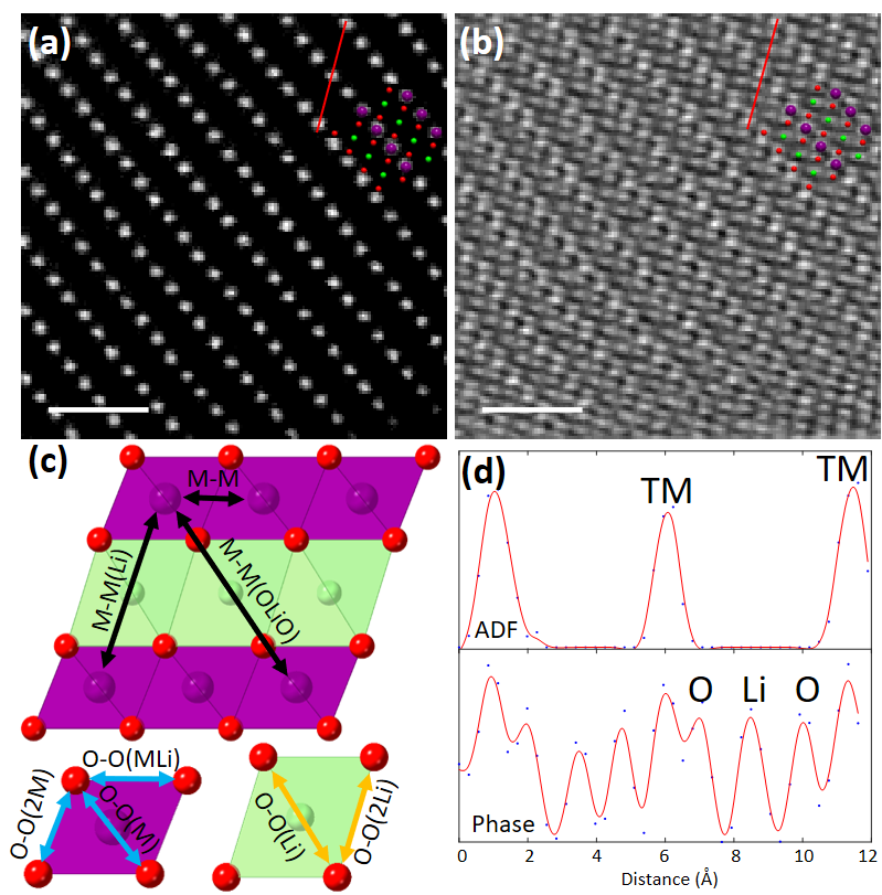
Figure 1 Measurement of projected atom distance in Li1.2[Ni0.13Mn0.54Co0.13]O2. Simultaneous (a) HAADF and (b) ptychographic phase image along [010] projection. Superposed is the crystal model, purple is TM, red O and green Li. Scale bar is 1 nm. (c) Illustration of atom distance. (d) Line profiles across the red lines in the HAADF and phase image. 

Uncaptioned visual

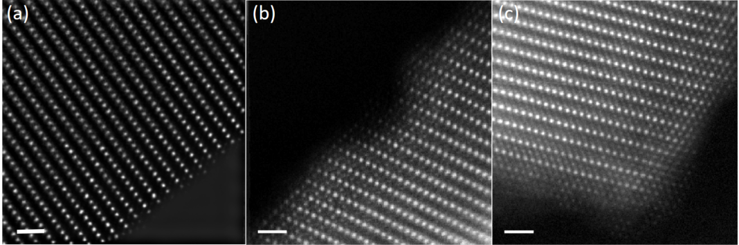
Figure 2 Atom distance measurement from zero-drift HAADF image of Li1.2[Ni0.13Mn0.54Co0.13]O2 at (a) pristine sate, (b) charged state and (c) discharged state. The dose is 3720, 2050 and 1943 e-2, respectively. Scale bar is 1 nm.  


Keywords

oxygen deformation; Li-ion battery; cathode; electron ptychography

References

[1] House, R. A. et al., Nature Energy 2020, 5 (10), 777-785.

[2] Liberti, E., et al., Ultramicroscopy 2019, 210, 112914.

[3] Lozano, J. G., et al, Nano Lett 2018, 18 (11), 6850-6855.

[4] Yang, H., et al, Ultramicroscopy 2017, 180, 173-179.

[5] Jones, L., et al, Advanced Structural and Chemical Imaging 2015, 1 (1), 8.

[6] The authors acknowledge use of characterization facilities within the David Cockayne Centre for Electron Microscopy, Department of Materials, University of Oxford and in particular the Faraday Institution (FIRG007, FIRG008), the EPSRC (EP/K040375/1 “South of England Analytical Electron Microscope”) and additional instrument provision from the Henry Royce Institute (Grant reference EP/R010145/1).


10:24 - 10:36

125 In situ EIS-TEM characterization of electrospun nanofibers for solid oxide electrolysis cells

Waynah Lou Dacayan1, Christodoulos Chatzichristodoulou1, Wenjing Zhang2, Kristian Mølhave3, Iram Aziz2, Søren Bredmose Simonsen1
1DTU Energy, Fysikvej, Kgs. Lyngby, Denmark. 2DTU Environment, Bygningstorvet, Kgs. Lyngby, Denmark. 3DTU Nanolab, Ørsteds Plads, Kgs. Lyngby, Denmark

Abstract Text

An in situ method allowing simultaneous structural and electrochemical investigation of solid oxide electrolysis cell (SOEC) nanofiber materials is developed for the latter’s thorough characterization. The method integrates electrochemical measurements, including Electrochemical Impedance Spectroscopy (EIS), to Transmission Electron Microscopy (TEM).

To achieve a stable supply of electricity from renewable sources, i.e. from solar and wind power, it is necessary to be able to store excess electricity for later use1,2. Through electrolysis, SOEC converts electrical energy to chemical energy that is suitable for storage, with high conversion efficiency. However, normally operated and most efficient at high temperature (800-1000°C)3-7, SOEC materials are prone to severe degradation which limits its use in the commercial scale. It is therefore important to improve the structural performance of the materials without sacrificing its good electrochemical response. This can only become possible if a full characterization of the materials can be acquired in its active state.

In this study, the SOEC nanofiber materials will be prepared through combining sol-gel synthesis and electrospinning. Based on our previous work and literatures, such ceramic nanofiber structure is capable to provide continuous ion conducting path, facilitate mass transports and enlarge triple phase boundaries (TPBs)8-10.

Using a MEMS based heating and biasing holder, the electrochemical and structural analysis of the materials will be done simultaneously inside an Environmental TEM. For the electrochemical analysis, I-V curves will be acquired in addition to EIS. During characterization, the materials will be exposed to high temperature, electrical potential, and reactive gases to simulate actual operating conditions.

The study will show the structural changes in the material as a function of temperature and time through TEM images. The associated I-V curves and EIS data will be presented, as well as the corresponding real time changes in conductivity as determined from the latter. These results will be correlated to show a complete picture of the materials’ response in an operating environment. The progress towards these goals will be reported.

Keywords

electrochemistry, solid oxide electrolysis cell, electrochemical impedance spectroscopy, electrospun fibers

References

[1] Laguna-Bercero M.A. Recent advances in high temperature electrolysis using solid oxide fuel cells: A review. Journal of Power Sources 203 (2012) 4-16. 

[2] Ebbesen S.D., Jensen S.H., Hauch A., and Mogensen M.B. High Temperature Electrolysis in Alkaline Cells, Solid Proton Conducting Cells, and Solid Oxide Cells. American Chemical Society (2014) 114, 10697-10734. 

[3] Elder R., Cumming D., and Mogensen M.B. High Temperature Electrolysis in Carbon Dioxide Utilisation: Closing the Carbon Cycle (2015) Chapter 11, pp. 183-209. 

[4] Zhang X., Song Y., Wang G., and Bao X. Co-electrolysis of CO2 and H2O in high-temperature solid oxide electrolysis cells: Recent advance in cathodes. Journal of Energy Chemistry 26 (2017) 839-853. 

[5] Yoon K.J., Son J.W., Lee J.H., Kim B.K., Je H.J., and Lee H.W. Performance and Stability of High Temperature Solid Oxide Electrolysis Cells (SOECs) for Hydrogen Production. ECS Transactions, 57 (1) 3099-3104 (2013). The Electrochemical Society. 

[6] Dönitz W. and Erdle E. High-Temperature Electrolysis of Water Vapor – Status of Development and Perspectives for Application. Int. J. Hydrogen Energy, Vol. 10, No. 5, pp. 291-295 (1985). 

[7] Hauch A., Jensen S.H., Ramousse S., and Mogensen M. Performance and Durability of Solid Oxide Electrolysis Cells. Journal of the Electrochemical Society, 153 (9) A1741-A1747 (2006). 

[8] Simonsen S.B., Shao J., and Zhang, W. Structural evolution during calcination and sintering of a (La0.6Sr0.4)0.99CoO3-δ nanofiber prepared by electrospinning. Nanotechnology, Vol. 28, No. 26 (2017).

[9] Ahn M., Seungwoo H., Lee J., and Lee W. Electrospun composite nanofibers for intermediate-temperature solid oxide T fuel cell electrodes. Ceramics International, Vol. 46, pp. 6006–6011 (2020).

[10] Parbey J., Xu M., Lei J., Espinoza-Andaluz M., Li T.S., and Andersson M. Electrospun fabrication of nanofibers as high-performance cathodes of solid oxide fuel cells. Ceramics InternationalVol. 46, Issue 5, pp. 6969-6972 (2020).


10:36 - 10:39

75 Nanoscale origins of degradation of Ni-rich NMC Li-ion battery cathodes

Mr Jedrzej Morzy1,2, Dr. Wesley Dose2,3, Amoghavarsha Mahadevegowda1,4, Clare Grey5,4, Prof. Michael de Volder2, Prof. Caterina Ducati1
1Dept. of Materials Science and Metallurgy, University of Cambridge, Cambridge, United Kingdom. 2Institute for Manufacturing, University of Cambridge, Cambridge, United Kingdom. 3Yusuf Hamied Dept. of Chemistry, University of Cambridge, Cambridge, United Kingdom. 4The Faraday Institution, Oxfordshire, United Kingdom. 5Department of Chemistry, University of Cambridge, Cambridge, United Kingdom

Abstract Text

Ni-rich cathode materials for Li-ion batteries such as LiNi0.8Mn0.1Co0.1O2 (NMC811) exhibit high volumetric and gravimetric specific capacities and low cost compared to other, isostructural materials with lower nickel content, which makes NMC811 a strong candidate for new generation of cathodes for Li-ion batteries. However, these layered transition metal oxides suffer from complex degradation mechanisms, where an interplay between lattice parameter changes during cycling, oxygen release at high states of charge, phase transformations at the surface, inter- and intragranular cracking, side reactions with electrolyte and transition metal (TM) dissolution all interact with each other, leading to capacity loss and impedance rise.1–3

Here, we use strategically designed electrochemical protocols (varying the time at high voltages, upper cut-off voltage, degree of (de)lithiation and number of cycles) aiming to decouple various degradation mechanisms. Based on full cell (NMC811/graphite) cycling data, coupled with area specific impedance from electrochemical impedance spectroscopy and hybrid pulse power characterisation, we show that the time at high voltages (even at 4.3 V) does not cause significant impedance rise, while the most severe cell capacity loss and impedance rise is present when the cells are cycled to >4.2 V during cycling. Moreover, capacity fade and impedance rise are also higher when the high upper cut-off voltage cycling is combined with large state-of-charge changes. 

To further investigate the impedance rise mechanisms, we complement the electrochemical data with electron microscopy of pristine and electrochemically stressed NMC811. We use scanning transmission electron microscopy ((STEM) imaging and electron energy loss spectroscopy (EELS) in a FEI Tecnai Osiris operated at 200 kV to probe the local, nanoscale structure and chemistry of NMC811 particles. Using a comprehensive data analysis approach, we report oxidation state evolution over cycling, where the average degree of TM reduction at the surfaces is correlated with the amount of impedance rise of the cells (in which the NMC811 cathode is the main contributor). Such behaviour points towards the surface reduced layer as the main culprit for impedance rise of NMC811/graphite cells. The EELS and electrochemistry results are supported by FIB-SEM tomography analysis of the samples. Pristine samples exhibit similar levels of cracking at secondary particle level as the cycled ones, which points to electrode manufacturing having a more significant impact on the cracking of NMC811 particles compared to their electrochemical history. 

In summary, by using tailored electrochemical protocols and advanced electron microscopy techniques, we identify the nanoscale changes in the chemistry of the surface layers as the main cause of impedance rise in NMC811/graphite cells. Using EELS, we find evolution of the chemistry of the surface reduced layer during cycling for the first time.  


Keywords

batteries, energy materials, EELS, STEM, FIB-SEM, focused ion beam, tomography, spectroscopy, cathode

References

1.        Kondrakov, A. O. et al. Charge-transfer-induced lattice collapse in Ni-rich NCM cathode materials during delithiation. J. Phys. Chem. C 121, (2017).

2.        de Biasi, L. et al. Chemical, Structural, and Electronic Aspects of Formation and Degradation Behavior on Different Length Scales of Ni‐Rich NCM and Li‐Rich HE‐NCM Cathode Materials in Li‐Ion Batteries. Adv. Mater. 31, 1900985 (2019).

3.        Jung, R., Metzger, M., Maglia, F., Stinner, C. & Gasteiger, H. A. Oxygen Release and Its Effect on the Cycling Stability of LiNixMnyCozO2 (NMC) Cathode Materials for Li-Ion Batteries. J. Electrochem. Soc. 164, A1361–A1377 (2017).


10:39 - 10:42

273 High energy resolution STEM-EELS as a powerful tool for the characterisation of battery materials

Angelica Laurita1, Jérémie Auvergniot2, Liang Zhu2, Pierre-Etienne Cabelguen2, Dominique Guyomard1, Nicolas Dupré1, Philippe Moreau1
1Université de Nantes, CNRS, Institut des Matériaux Jean Rouxel, IMN, 2 rue de la Houssinière, F-44000 Nantes Cedex 3, France. 2Umicore, Rechargeable Battery Mat, 31 Rue Marais, BE-1000 Brussels, Belgium

Abstract Text

The electrification of vehicles presently relies on lithium ion batteries using layered oxides of nickel, manganese and cobalt (NMC) with high Ni content as positive electrode materials. Nevertheless, it has been demonstrated that these materials suffer from gassing issues decreasing cycle life and causing safety problems. Moreover, nickel-rich NMCs are affected by critical instability during all the manufacturing steps (synthesis, handling, electrode preparation). A deep comprehension of the pristine material properties and of its behaviour during electrode preparation and electrochemical cycling is thus fundamental from the industries’ point of view.

In this context a systematic study of the surface reactivity of NMC811 (Li[Ni0.8Mn0.1Co0.1]O2) was conducted using a multi-analytical approach in which transmission electron microscopy plays an essential role. A new TEM/STEM Themis Z G3 (Thermo Fisher Scientific) equipped with a double camera GIF spectrometer, was recently installed in the Jean Rouxel Institute of Materials of Nantes (France). Electron Energy Loss Spectroscopy (EELS) was in particular exploited in order to give a complete description of the surface of the material.

The direct detection camera (Gatan K2 Summit) allowed the acquisition of EELS spectra in STEM mode with both high energy and spatial resolution. This enables a good multi-elemental chemistry mapping quantification (at low energy dispersions) as well as the accurate analysis of the fine structures of the Ni L23 -edges thanks to the use of an excited monochromator. Moreover, the use of a vacuum transfer sample holder insured the observation of samples without any contact with the ambient atmosphere. The samples were in fact transferred directly to the microscope from the Argon glove box where they were stored, preventing any sort of reaction of the material with air and thus allowing the proper analysis of the material in its initial state.

In this way it was possible to look at the surface modifications and to compare them to the bulk structure by means of both the multiple linear least square (MLLS) fitting and the Principal Components Analysis (PCA); the thickness of the surface modified layer was then determined for all the samples, proving the high reactivity of the material surface in humid atmosphere. The Ni L3-edge changes in fact between the surface and the bulk of the material, indicating its oxidation state’s evolution after 2 days in 30% of Relative Humidity. The reduced Ni was found for about the first 15 nm of the surface. 

On the other hand, the analysis of the same powder transferred directly from the glove box revealed a similar behaviour of the Ni L-edge (Figure 1) in the first 6 nm of surface only; a slight change in the 

Uncaptioned visual

Figure 1: Evolution of Ni L3-edge in the pristine NMC 811 powder


shape of the oxygen K-pre-edge was also observed, indicating that a gradual but not yet completed evolution of the material surface.

Moreover, through the calculation of the second derivative of the EELS spectra, a quantification of all the transition metals was performed. It has to be considered here that the small quantity of Mn and Co in the material doesn’t usually allow the correct quantification of these species, since the corresponding intensity signal is too low and often confused into the background. For this reason, changes in the surface composition of this materials have rarely been deduced by EELS spectra at this level of precision.

Uncaptioned visual

Figure 2: STEM-EELS Zero-Loss Peak intensity on a FIB lamella of a NMC811 secondary particle


In addition to primary particle analysed above, FIB lamellas (Figure 2) were also produced on secondary particles (made of these primary particles) actually used by our industrial partner. First results on these closer to application samples will be presented so that we can demonstrate how the observed phenomena on primary particles translate at a larger scale. 

To conclude, EELS Spectrum Images were analysed in order to obtain qualitative and quantitative information about the surface of NMC811, essential to the good comprehension of its reactivity and gassing behaviour. EELS was used for the determination of both the valence state, coordination and quantity of all the transition metals as well as for the qualitative identification of surface modifications in particular aging conditions.


10:42 - 10:45

117 Electrochemical TEM experiments on solid oxide electrolysis cells

Zhongtao Ma1, Kristian Mølhave2, Christodoulos Chatzichristodoulou1, Søren Simonsen1
1Department of Energy Conversion and Storage, Technical University of Denmark, Fysikvej, 2800 Kgs. Lyngby, Denmark. 2National Centre for Nano Fabrication and Characterization, Technical University of Denmark, Fysikvej, 2800 Kgs. Lyngby, Denmark

Abstract Text

In this work, in situ transmission electron microscopy (TEM) and in situ electrochemical impedance spectroscopy (EIS) are combined, to directly correlate structural and chemical evolution of the cell components with electrochemical properties of solid oxide electrolysis cells (SOEC).

Hydrogen production and application from electrolysis will play a vital role in future energy systems, such as the transportation and energy storage sector. Regarding electrolysis, solid oxide electrolysis cell (SOEC) technology has been reported as the most suitable option for wide-scale adoption [1]. Gadolinium doped ceria (CGO) with decent ionic conductivity is currently used as a barrier layer, and yttrium stabilized zirconia (YSZ) is used as the electrolyte in state-of-the-art SOEC [2][3]. However, degradation at the CGO-YSZ interface has a large contribution to the degradation of the electrolysis cell [4]. In order to improve the performance of the CGO-YSZ interface and optimize the CGO and YSZ themselves, we need to determine the relations of the electrochemical activity and structure/composition. 

In this work, in situ transmission electron microscopy (TEM) and in situ electrochemical impedance spectroscopy (EIS) are combined together, which allows the study of nanostructure development of cells at elevated temperature and electrode polarization conditions in a reactive gas environment.

An optimal procedure for handling, mounting, and conducting experiments with the model cells has been developed. A nano-sized symmetrical cell with CGO (electrode, 100 nm)-YSZ (electrolyte, 100 nm)-CGO (electrode, 100 nm) is synthesized by pulsed laser deposition (PLD), and followed by a focused ion beam (FIB) process. MEMS chips developed at DTU Nanolab and commercial MEMS chips are used to achieve the application of the electrical potentials and elevated temperatures. The electrochemical properties are evaluated as a function of different temperatures and gas compositions.

We can increase the electrical polarization while observing changes in crystal phases and morphology at the CGO-YSZ interface. For example, we can follow the oxidation state of cerium in CGO changing as a function of distance to the CGO-YSZ interface and as a function of applied bias. Possible new phase formation, element segregation, and some failure contributors like voids and cracks generated along the interface can also be determined. The goal of this project is not only to solve a specific scientific problem but also to provide a platform that can establish relations between nanostructures and electrochemical properties.


Keywords

in situ; transmission electron microscopy (TEM); electrochemical impedance spectroscopy (EIS); solid oxide electrolysis cells (SOEC); gadolinium doped ceria (CGO); yttrium stabilized zirconia (YSZ)

References

[1] Hauch, Anne, et al. "Recent advances in solid oxide cell technology for electrolysis." Science 370.6513 (2020).

[2] Ebbesen, Sune Dalgaard, et al. "High temperature electrolysis in alkaline cells, solid proton conducting cells, and solid oxide cells." Chemical reviews 114.21 (2014): 10697-10734.

[3] Garbayo, I., et al. "Full ceramic micro solid oxide fuel cells: towards more reliable MEMS power generators operating at high temperatures." Energy & Environmental Science 7.11 (2014): 3617-3629. 

[4] Tietz, F., et al. "Degradation phenomena in a solid oxide electrolysis cell after 9000 h of operation." Journal of Power Sources 223 (2013): 129-135.


10:50 - 11:02

150 The atomic-scale microstructure of metal halide perovskites elucidated via low-dose scanning transmission electron microscopy

Dr Mathias Uller Rothmann1,2, Dr Judy Kim2,3,4, Dr Juliane Borchert1, Kilian B. Lohmann1, Dr Colum M. O'Leary2, Alex A. Sheader2, Dr Laura Clark2, Professor Henry J. Snaith1, Professor Michael B. Johnston1, Professor Peter D. Nellist2, Professor Laura M. Herz1
1University of Oxford, Department of Physics, Oxford, United Kingdom. 2University of Oxford, Department of Materials, Oxford, United Kingdom. 3ePSIC, Diamond Light Source, Harwell, United Kingdom. 4Rosalind Franklin Institute, Harwell, United Kingdom

Abstract Text

Understanding the atomic-scale crystallographic properties of photovoltaic semiconductor materials such as silicon, GaAs, and CdTe has been essential in their development from interesting materials to large-scale energy conversion industries. However, studying photoactive hybrid perovskites by transmission electron microscopy (TEM) has proved particularly challenging due to the large electron energies typically employed in these studies.[1] In particular, the very close structural relationship between a number of crystallographic orientations of the pristine perovskite and lead iodide has resulted in severe ambiguity in the interpretation of EM-derived information, severely impeding the advance of atomic resolution understanding of the materials.

Here, we successfully image the archetypal CH(NH2)2PbI3 (FAPbI3) and CH3NH3PbI3 (MAPbI3­) hybrid perovskites in their thin-film form with atomic resolution using a carefully developed protocol of low-dose STEM.[2] Our images enable a wide range of previously undescribed phenomena to be observed, including a remarkably highly ordered atomic arrangement of sharp grain boundaries and coherent perovskite/PbI2 interfaces, with a striking absence of long-range disorder in the crystal. These findings explain why inter-grain interfaces are not necessarily detrimental to perovskite solar cell performance, in contrast to what is commonly observed for other polycrystalline semiconductors. Additionally, we observe aligned point defects and dislocations that we identify to be climb-dissociated, and confirm the room-temperature phase of CH(NH2)2PbI3 to be cubic. We further demonstrate that degradation of the perovskite under electron irradiation leads to an initial loss of CH(NH2)2+ ions, leaving behind a partially unoccupied, but structurally intact, perovskite lattice, explaining the unusual regenerative properties of partly degraded perovskite films. Our findings thus provide a significant shift in our atomic-level understanding of this technologically important class of lead-halide perovskites.


Keywords

Perovskite solar cells, atomic-resolution, STEM, low-dose

References

[1] Adv. Mater. 2018, 30, 1800629

[2] Science 370, eabb5940 (2020)


11:02 - 11:14

92 Understanding Cu-Alumina interactions in redox conditions for Chemical Looping Combustion (CLC) application – A multi-scale correlative electron and X-ray microscopy study

Sharmin Sharna1,2, Virgile Rouchon1, Anne-Lise Taleb1, Christèle legens1, Stefan Stanescu3, Arnold Lambert1, Anne-Sophie Gay1, David Chiche1, Ovidiu Ersen2
1IFP Energies nouvelles, Lyon, France. 2Institut de Physique et de Chimie des Matériaux de Strasbourg, Strasbourg, France. 3Synchrotron Soleil, Gif-sur-Yvette, France

Abstract Text

Chemical Looping Combustion (CLC) is a midterm solution for fossil fuel utilization with inherent carbon dioxide capture, based on the use of an oxygen carrier material. The oxygen carriers (OC) replace air to provide oxygen to a wide range of fuels for combustion, via reduction/oxidation cycles in a circulating fluidized bed reactor at high temperature [1]. Copper oxide supported on alumina grain (CuO/Al2O3) has been widely considered as a promising oxygen carrier (OC) for industrial use in CLC, due to its benign nature and flexible redox behavior that ensures high reactivity and oxygen transfer capacity. However, the OC sustains successive high temperature (800-900°C) reduction (combustion) and oxidation (regeneration of oxide phase) reaction cycles which lead to chemical and morphological changes in the material causing the degradation in the oxygen carrying properties. The evolution in the cycled material is attributed to the diffusion of the Cu-based phases at the grain scale [2].

Herein, we are bridging the gap in understanding between the observed μm-scale migration of Cu-based phases and nanoscale transformations of the Cu nanoparticles (NPs) by employing a multi-scale characterization approach using Scanning Transmission X-ray (STXM) and Scanning Transmission Electron (STEM) Microscopies, respectively. Correlative spectro-microscopy is used to characterize the evolution of interacting Cu and Alumina phases after different aging times under successive redox cycles. Furthermore, in-situ STEM, mimicking redox cycling, is used to achieve a nanoscale view of the phase/morphological evolution of the Cu NPs and to identify the sintering mechanism of the copper phases during successive reduction and oxidation steps.

We have studied CuO phase supported on 50-100 µm sized γ-Al2O3 grain, produced via incipient wetness impregnation of 13%wt CuO and calcined at 800 °C. To mimick the CLC cycling, the fresh samples were subjected to oxidation and reduction under air and Hat 900 °C, in a thermogravimetric analyser (TGA). Ultramicrotomy sections of 100 nm thickness of were prepared for SEM, STXM and TEM characterizations. STXM was performed at the HERMES beamline of the Soleil Synchrotron facility. Energy stacks and mappings were performed at the Cu L-edge and Al K-edge in order to identify the specific spectral features of each compound and to map their distribution with ~40 nm resolution. Using external standards of CuO, Cu(II) aluminate (CuAl2O4), γ and α-Al2O3, spectral features at 934 eV, 933 eV, 1579 eV and 1581 eV were representative of each phase respectively. In-situ TEM was performed using a probe Cs-corrected microscope equipped with Protochips’ ”Atmosphere” in-situ gas setup with sealed environmental cell (E-Cell), operating at atmospheric pressure.

The fresh grains are composed of γ -Al2O3 with homogeneously dispersed CuO nanoparticles (10-20 nm) and large (µm sized) CuO particles on the outskirts of the grain. With progressive cycling, at the grain scale (µm), we observe the disappearance of the large CuO particles and the propagation of a gamma to alpha reaction front in the solids (Figure 1). At smaller scale (10 x 10 µm2), this front displays a well-defined structural-chemical gradient characterized by (figure 2b): zone 1, non-stoichiometric Cu (II) aluminate; zone 2, an intermediate thin layer (< 200 nm) of Cu (II) aluminate, enriched in Cu compared to zone 1; zone 3, α-Al2O3 phase containing large CuO particles. The proportion of copper shows a strong variation from 10 wt% Cu in zone 1, to ~25wt% at the edge of the reaction front in zone 2. In zone 3, copper is concentrated in localized particles of several tens of nm in diameter indicating a strong sintering effect.


Uncaptioned visual

In-situ STEM observation at 900 °C under H2-reduction have shown the migration of copper to form copper nanoparticles from a starting oxidized sample mainly composed of homogeneous Cu (II) aluminate (Figure 2). It is suspected that the expelling of Cu from the spinel structure of Cu (II) aluminate favors the formation of the corundum structure of Cu-free Al2O3. This suggests that the mobility of copper during redox cycling is linked to the phase transition of γ- to α-Al2O3. However, the γ- to α-Al2O3 transition is not favored in the pure Al-O system below 1000 - 1100 °C [3]. Reversely, the oxidative formation of spinel is only possible in the CuO+γ-Al2O3 system and thermodynamically limited in the case of CuO+α-Al2O3, at 900 °C [4]. To minimize the energy of the system, the mobility of copper on alumina during oxidation is sufficient to either form (1) CuAl2O4 at the expense of g-Al2O3, and (2) larger CuO particles on α-Al2O3 by sintering. Through a step by step migration mechanism induced by the redox cycling, copper is being gradually concentrated at the external border of zone 3, the latter expanding through the grains until reaching complete a-Al2O3 formation. Fractions of copper not being able to reach γ-Al2O3 particles during an oxidation cycle sinter to form larger, more stable particles on the α-Al2O3 surface.

 Uncaptioned visual
This study demonstrates how correlative multi-scale imaging techniques can be employed to reveal the dynamic interactions of metal/metal oxides and ceramic supports in complex reactive systems.


Keywords

Chemical Looping Combustion, CLC, Oxygen Carrier, Copper Oxide, Copper, CuO-Alumina, Oxidation-Reduction, in-situ STEM, STXM-XAS, Correlative microscopy 

References

[1] Adanez et al., Progress in Energy and Combustion Science, 38, (2012), 215-282
[2] Lambert et al., Fuel, 216 (2018), 71–82
[3] Boumaza et al., Journal of Solid State Chemistry, 182 (2009) 1171–1176
[4] Hu et al., RSC Advance, 6 (2016),113016–113024


11:14 - 11:17

108 Structure-property Correlation of Black ZnO Nanoparticles with High Absorbance for Photovoltaic Applications

Praveen Kumar1, Paul Brunet2, Davide Mariotti2, Miryam Arredondo1
1Centre for Nanostructured Media, School of Mathematics and Physics, Queen’s University Belfast, BT1 7NN, Belfast, United Kingdom. 2Nanotechnology and Integrated Bio-Engineering Centre (NIBEC), Ulster University, Newtownabbey BT37 0QB, Belfast, United Kingdom

Abstract Text

ZnO has been widely studied for its numerous applications in optoelectronic devices, biomedical science, surface plasmons, sensors, photocatalysis, and photovoltaic solar cells [1−2]. ZnO has a wide bandgap semiconductor material (3.3 eV at room temperature) with a large exciton binding energy of 60 meV which makes it suitable for a variety of optoelectronic applications [1−2]. An interesting research aspect is the defect formation and non-stoichiometry (Zn interstitials, O vacancies or vice versa) associated with ZnO . It is widely accepted that non-stoichiometric ZnO produces n-type conductivity, but the subject remains controversial as recent studies have reported that the addition of hydrogen in ZnO can act as a shallow donor and could be responsible for the n-type character [3−6]. The large bandgap of ZnO (showing absorption in the ultraviolet region) limits its ability to absorb visible light which could be harvested for photovoltaic applications. However, due to its tunable nature, alloying or doping ZnO with other dopant materials can promote novel electronic and optical properties by introducing defects energy levels within the bandgap. Moreover , a metal /ZnO core-shell approach has been proposed as an alternative route to control optical properties by incorporating structural disorder [7]. More recently, Xiu et al. have synthesized hydrogenated black ZnO nanoparticle with improved absorption and photocatalytic performance [8]. Thus, introducing defects in a controlled manner allowing for tuning optical and electronic properties that can drive important reactions or drastically increase absorption, while several of the advtantages of metal oxides can be preserved.

Using a plasma-based technique [9], we have been able to produce Zn-based nanoparticles black in appearance. Nanoparticles were deposited on a Si substrate and the resulting absorption characteristics are very distinct from ZnO. As-synthesized nanoparticles showed very low transmittance across the spectral range and high absorbance over large wavelength regions (300−1400 nm, see Fig. 1f). Thus, this study aims to understand the crystal and electronic structure responsible for this high absorption. 

The morphology, structure, and crystallinity of ZnO nanoparticles were investigated by transmission electron microscopy (TEM) techniques, performed on a Thermo Fisher Talos F200X G2 in TEM mode operated at 200 kV and equipped with a FEG (field emission gun) cathode and four in-column Super-X energy dispersive X-ray spectrometer (EDS) detectors having a total collection angle of ∼0.9 sr. Qualitative chemical analysis of ZnO nanoparticles was determined by energy-dispersive X-ray spectroscopy (EDX) in STEM mode. 

An exemplary bright-field TEM image of ZnO nanoparticles is presented in Fig. 1a. The nanoparticles are of irregular shapes with no clear morphology, rather a variety of shapes such as hexagonal, square, and rectangular with size ranging from 15−50 nm. The corresponding selected area electron diffraction (SAED) pattern revealed several diffraction rings (see Fig. 1b). The diffraction rings were indexed with ZnO wurtzite (hexagonal) and Zn hexagonal structures, indicating the formation of a mixed phase. Center dark-field images (CDF) using the (101) reflection of wurtzite ZnO (not shown here) show nanoparticles that are strongly excited due to diffraction contrast providing a sense of phase distribution. More interestingly, we noticed a clear contrast at the edges of the nanoparticles which suggest a possible two-phase material or a core-shell structure.

To further verify this, we performed STEM-EDX elemental mapping of ZnO nanoparticles as shown in Fig. 1c. Qualitatively, color mix image (Zn (magenta) and O (green)) clearly showed the presence of a core-shell structure. We noticed a slightly higher oxygen count (follow green regions, Fig. 1c) in the shell region as compared with the core part of the nanoparticle. The thickness of the shell was estimated in the range of 2-4 nm. Fig. 1d displays the STEM-EDX line profile across the nanoparticle (see the arrow, Fig. 1d). It is evident from the line profile that O counts are higher in the shell areas and lower in the core part of the nanoparticle. Thus, by combining dark-field imaging and STEM EDX measurements, we can confirm the core-shell nature of ZnO nanoparticles. Quantitative chemical composition was also investigated by XPS (not shown here) on the as-synthesized nanoparticles yielding Zn (65 at.%) and O (35 at.%) atomic concentrations.

High-resolution TEM images were acquired to confirm the crystallinity, defects, and structural disorder in ZnO nanoparticles. In accordance with the SAED results, we observed more complex lattice fringes (not shown here) within individual particles that match well with both ZnO and metallic Zn phases, indicating that the nanoparticles are not single-crystalline. Interestingly, we noticed some hints of long-range ordering/structural disorder (in Fig. 1e) with spacings of about 1.33 nm, which is a typical signature of oxygen deep level defects as recently reported by Chen et al. on the α-Fe2O3 nanowires [10].

The findings of this study strongly suggest that black ZnO nanoparticles could be utilized for photovoltaic applications due to their exciting optical properties and tunability. The absorption results are very distinct from the typical ZnO. At this stage of understanding, our structural analysis suggests possible explanations for this high absorption that could be related to; (i) the formation of the core-shell structure, (ii) mixed-phase of Zn and ZnO wherein the shell is slightly rich in oxygen as compared with the core part of the nanoparticle, and, (iii) defects presence:  long-range ordering due to oxygen vacancies or stacking faults. This off stoichiometric in the core-shell region resulting in a disordered structure that could be responsible for this high absorption. Further studies on ZnO nanoparticles, particularly, the atomic resolution electron microscopy work need to be carried out to address the ZnO/Zn interface defects to validate and understand the heuristic mechanisms which lead to enhanced optical properties. 

Uncaptioned visual

Figure. 1: (a) Overview bright-field image of ZnO nanoparticles and, (b) the corresponding SAED pattern. (c-d) STEM-EDX elemental mapping of Zn and O revealing a core-shell structure and corresponding line profile. (e) HRTEM image showing spacings of 1.33nm which could be related to long-range ordering or due to oxygen vacancies. (f) Optical measurements of ZnO nanoparticle exhibiting a high absorption over a large wavelength region.

Keywords

ZnO, Nanostructure, metal oxide semiconductor, defects, Transmission Electron Microscopy

References

  1. Ü. Özgür et al., J. Appl. Phys., 98, 2005, 041301.
  2. S. T. Kochuveedu et al., Chem. Soc. Rev., 42, 2013, 8467.
  3. A. Janotti et al., Phys. Rev. B., 76, 2007, 165202-22.
  4. D. C. Look et al., Phys. Rev. Lett., 82, 1999, 2552-2555.
  5. E. Ziegler et al., phys. stat. sol. (a), 66, 1981, 636.
  6. C. G. Van de Walle, Phys. Rev. Lett., 85, 2000, 1012-1015.
  7. H. Zeng, et al., J. Phys. Chem. B, 111, 2007, 14311-14317.
  8. T. Xia et al., RSC Adv., 4, 2014, 41654.
  9. G. Jain et al., Nanotechnology, 31, 2020, 215707.
  10. Z. Chen et al., Chem. Mater., 20, 2008, 3224–3228.

11:17 - 11:20

107 Understanding the degradation of Be tiles in the JET tokomak reactor using EELS and DFT

Mr. Xinlei Liu, Ms. Carmen Makepeace, Dr. Rebecca Nicholls, Prof. Sergio Lozano-Perez, Prof. Jonathan Yates
University of Oxford, Oxford, United Kingdom

Abstract Text

Beryllium metal is used as a plasma-facing component for the International Thermonuclear Experimental Reactor (ITER) first wall due to its limited reactivity with hydrogen isotopes and good oxygen gettering ability [1]. In the Joint European Torus (JET) tokamak, beryllium tiles are subject to both power and particle loads [2]. The erosion involves 2 major mechanisms: formation of oxides over its surface when exposed to air and deuterium retention during the co-deposition of hydrogen isotopes with beryllium atoms from the edge plasma [3].

To understand the corrosion mechanism of the materials, it is vital to discover the structures of the corrosion products. However, the exact structure cannot be determined from diffraction methods as the selected beryllium oxide area involves more than one structure. In this work, we use a combination of experimental and simulated electron energy loss (EEL) spectra to determine the reaction produces. EEL spectra, both in the low-loss and core-loss regime, of seven candidate structures Be, BeH2α-Be(OH)2β-Be(OH)2α-BeO, β-BeO, and BeO2 are calculated using density functional theory (DFT). For each structure, we performed three calculations: lowloss, Beryllium K-edge and Oxygen K-edge of EEL spectra. The DFT calculations have been performed using the CASTEP code [4]. The PBE functional was selected and ultrasoft pseudopotentials were used in the calculations. 

Uncaptioned visual              Uncaptioned visual

         (a)                                                                                                         (b)

Uncaptioned visualUncaptioned visual

                                                (c)                            (d)

Figure 1: (a) STEM image showing region of EDX maps of an as-received JET Be sample, unexposed to H plasmas. (b) Experimental Be K-edge EEL spectra of the sample. (c) Simulated Be K-edge of EEL spectra of beryllium metal. (d) Simulated Be K-edge of EEL spectra of α-BeO (Hexagonal) 

As shown in Figure 1, there are distinctive features in the EEL spectra simulated for different materials. By comparing calculated and experimental EEL spectra, we see features proving the existence of Be metal and polymorphs of BeO. EEL spectrum at point 8 matches the simulated one of Be metal while EEL spectrum at point 1 corresponds to α-BeO (Hexagonal). Further confirmation was done for the oxygen K-edge and the low-loss EEL spectra.  

The simulated spectra are compared with five sets of experimental data: standard, as-received, deposited, eroded, and melted. The standard samples were used as bench marks to verify if the simulated results were accurate. The as-received sample corresponded to a piece of beryllium metal which was not subjected to any nucleation reactions and corroded at room temperature. The remaining three samples came from different parts of JET tokamak. When comparing the simulated and experimental results, shapes and relative positions of the peaks of EEL spectra of different materials were used to identify the exact structure of the samples.  


Keywords

JET tokomak reactor, degradation of beryllium, EELS, DFT

References

  • [1] Beal, J. M. (2016). Erosion, deposition and material migration in the JET divertor with carbon and ITER-like walls. University of York.
  • [2] Roth, J., Doerner, R., Baldwin, M., Dittmar, T., Xu, H., Sugiyama, K., Reinelt,M., Linsmeier, Ch., Oberkofler, M. (2013). Oxidation of beryllium and exposure of beryllium oxide to deuterium plasmas in PISCES B. Journal of Nuclear Materials, 438, S1044–S1047. 
  • [3] Makepeace, C., Pardanaud, Roubin, P., Borodkina, I., Ayres, C.,  Coad, P., Baron-Wiechec, A.,  Jepu, I., Heinola, K., Widdowson, A., Lozano-Perez, S., J.E.T. Contributors (2019). The effect of Beryllium Oxide on retention in JET ITER-like wall tiles. Journal of Nuclear Materials, 19, 346-351.
  • [4] Clark, S. J.; Segall, M. D.; Pickard, C. J.; Hasnip, P. J.; Probert, M. J.; Refson, K.; Payne, M. C. (2005). First principles methods using CASTEP, Zeitschrift fuer Kristallographie, 220 (5-6), 567-570