14:15 - 14:45
Vibrational spectroscopies offer of the ability to interrogate chemical bonds directly. Conventionally used IR and Raman spectroscopies probe molecular vibrations and phonons in large materials volumes, capturing details of functional groups and lattice dynamics, while tip-enhanced scanning near-field implementations have enabled vibrational spectroscopy approaching 10 nm spatial resolution but limited to surface studies. Recent advances in electron energy loss spectroscopy in the scanning transmission electron microscope (STEM-EELS) have enabled the observation of the spectral signatures of phonons and molecular vibrations at much shorter length scales. In molecular systems, where long range interactions have enabled ‘aloof’ spectroscopy with reduced electron beam induced damage, the broadband energy window accessible in high resolution EELS also makes it possible to detect the optical signatures from the mid-infrared to the UV energy range. However, understanding variations in bonding or optical response at the nanoscale in molecular and metal-organic solids requires measurements with higher spatial sensitivity than afforded by the simple aloof beam approach. Here, we develop strategies for high spatial and energy resolution STEM-EELS to fingerprint the optical properties and molecular vibrations of beam-sensitive organic materials at the nanoscale.
Organic and metal-organic framework (MOF) glasses show significant promise in applications from LEDs and photovoltaics to photocatalysis but their macroscopic optoelectronic properties are often only linked to microscopic optical properties and atomic structure in statistical descriptions of volumes much larger than the molecule or unit cell. In contrast, high-energy-resolution STEM-EELS provides a nanoscale fingerprint of these optical properties and of characteristic molecular vibrations in MOFs. In particular, as a result of tetrahedral ligand-field splitting at Co metal centres, d-d transitions directly reflect the local coordination [1] , while intra-ligand and metal-to-ligand transitions in the vibrational signal can be mapped with nm precision to distinguish nanoscale regions of distinct coordination chemistry. [2]
Meteoritic samples with organic inclusions, such as carbonaceous chondrites, are of particular importance in the study of ancient organic compounds that may have served as precursors for the prebiotic history of the early Earth. In order to elucidate the functional chemistry of these materials and understand the complex processes of formation and consecutive alterations they might have undergone in the early solar nebula, we use monochromated STEM EELS measurements at low acceleration voltage and controlled beam current. These conditions below the C knock-on damage threshold and with reduced electron doses, allow for the detailed observation of the pristine chemistry of the organics; vibrational EELS measurements alongside the carbon and nitrogen near edge fine structures (ELNES) reveal the presence of different functional groups, namely aliphatic and carboxyl bonds, on a submicron scale which can be attributed to early cometary and meteoritic organic reservoirs. [3,4]
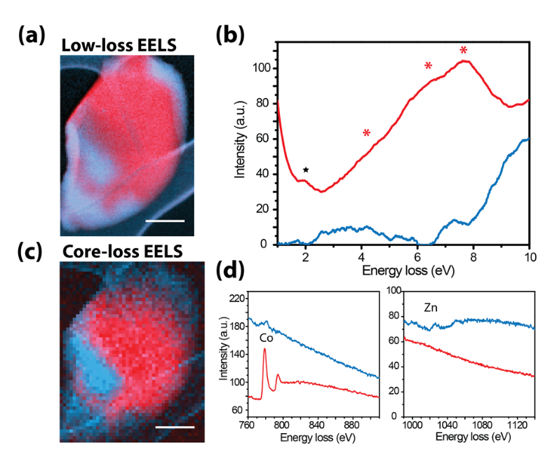
Figure 1. Low- (a-b) and core- loss (c-d) STEM measurements of zeolitic imidazolate (ZIF) metal-organic framework glass blend. Panel (a) shows superimposed coloured maps generated by non-negative matrix factorization (NMF) applied on low loss EELS data, while the corresponding spectral factors are illustrated in (b). The method is used to directly visualise the d-d transitions at Co metal centres (marked by * in (b)), reflecting the local tetrahedral ligand-field splitting. Panel (c) shows superimposed maps of Co and Zn of the same particle, generated by independent component analysis (ICA) from coreloss EELS data (d). The scale bars are 300 nm. Adapted from [1].
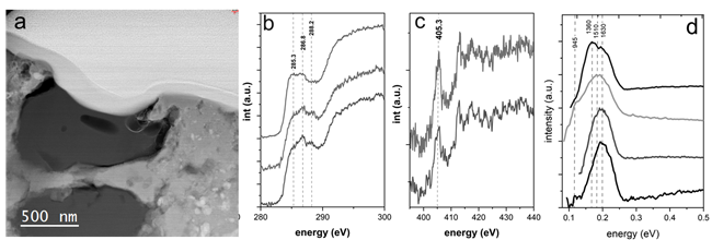
Figure 2. (a) High Angle Annular Dark Field (HAADF) STEM image of an organic inclusion in the Renazzo carbonaceous chondrite. (b,c) monochromated core-loss measurements of the C K and N K ionization edges highlighting several spectral bands characteristic of the organic functional chemistry of the inclusion, including ketone/aldehyde/nitrile and carboxylic bonding and possible nitrate groups. (d) Vibrational EELS measurements; two major bands at around 1360 cm-1 and 1630 cm-1 can be identified, which relate to the D- and G-bands of amorphous carbon. The peak positions on different regions within the grain vary on a nanometer scale, most likely due to the heterogeneous nature of the organic matter. Adapted from [3].
STEM, EELS, vibrational spectroscopy, beam sensitive materials, MOF, meteorites
14:45 - 14:57
Polyamide reverse osmosis (RO) membranes are used on offshore platforms for seawater desalination. These membranes typically consist of a polyester backing layer, a 60-100 μm polysulfone (PSf) support film and a 100-700 nm thick polyamide (PA) film. This layered RO membrane has a complex structure with the tight PA separation layer containing porosity or density modulations on the nanoscale which control salt and ion selectivity. However, the structure of the PA layer and its contribution to ion selectivity, is poorly understood.
Whilst neutron reflectivity [1] and scanning transmission x-ray microscopy (STXM) [2] have been used to probe polymer membranes with high spatial resolution in the z direction and high energy resolution respectively, the only technique that is able to map functional chemistry with nanometre spatial resolution, is scanning transmission electron microscopy (STEM) combined with electron energy-loss spectroscopy (EELS). Recent advances in monochromators mean it is now possible to perform spatially resolved EELS with energy resolutions matching those of X-ray absorption spectroscopy.
Soft materials, such as polymers, are particularly challenging to study in the TEM due to the very low characteristic electron dose (characteristic electron fluence) required before damage occurs to the chemical bonds [3]. As a result, acquiring spatially resolved data in beam sensitive samples, is non-trivial. Here we present spatially resolved EELS maps with a resolution of <10 nm across PA membranes.
First, we carried out control beam damage experiments investigating the effect of parameters such as acquisition time, pixel size, sub-pixel scanning and probe size on the C K edge fine structure of plan view PA membranes. The membranes had a nominal thickness of 12 nm and data was acquired from an area of 800 x 800 nm2. Acquisition from such a large area allows lower doses to be used and the signal to be summed to improve the signal-to-noise ratio. This work was carried out at SuperSTEM on a Nion UltraSTEM 100MC “HERMES” monochromated electron microscope operated at 100 kV with a STEM probe size of 0.9 Å.
To investigate the effect of acquisition time/electron dose on the signal, a pixel spacing of 5.3nm was used and the acquisition time varied between 0.01-0.12 s, corresponding to an electron fluence of 7.03 – 42.2x 10⁶ e/Å2. Electron fluences described here were calculated as a function of probe size rather than pixel size resulting in an increase of three orders of magnitude compared with those reported elsewhere. With a 0.02 s acquisition time three clear, sharp peaks were observed in the π* region of the C K edge at ~285.1, 286.4 and 288.0 eV. As the dwell time was increased peaks 1 and 3 reduced in intensity. Peak 1 moving to higher energy-loss and all three peaks merged forming one broad peak at around 286-288 eV. At this dose none of the features in the π* region can be distinguished. There was indication that a critical dose had been reached at an acquisition time of 0.02 s.
The influence of probe size was also investigated, comparing a probe of 0.09 nm with 1 nm whilst maintaining a pixel spacing of 5.3 nm. It was found that although the larger probe had a lower electron fluence, it actually caused more damage to the spectra. This indicates that the damage extends a significant distance from the probe position itself. To investigate this further the spacing between pixels was varied and data recorded for pixel sizes between 1 - 5.5 nm. For the same probe size and dose, the closer together the pixels the more damaged the spectra. This confirms that significant damage occurs outside of the electron probe such that when the electron beam probes the adjacent pixel its chemistry has already been altered.
Similar damage experiments were carried out for the resin and PSf. Whilst some changes in fine structure were observed, the large effects seen for PA were not there suggesting these polymers were already significantly chemically damaged at the electron fluences used for this study.
These studies are useful and essential. However, when probing chemical pathways across the depth the of the PA membrane i.e. in cross section, there is very little area from which to sum spectra to achieve high enough signal-to-noise ratio. Additionally, to observe changes in chemistry with sub-nm spatial resolution, as already discussed, the increased spectral damage can be significant. The dose required to achieve sufficient signal-to-noise ratio with this kind of spatial resolution, undoubtedly damages the chemical bonds. However, in this study we found that despite some damage and broadening observed in the C K edge, and in addition to mapping the elemental distribution, it is still possible to map spatial variation in functional chemistry across the membranes by integrating over windows corresponding to the main peaks found in the reference, minimally damaged spectra. Non-negative matrix factorization (NMF) machine learning algorithms were also used to gain further insights into the chemistry of the PA layer showing clear localisation of signal suggesting that the maps are representative of specific and real functional chemistry within the PA, PSf and resin layers.
In conclusion, it was found that by comparison with carefully acquired reference data it was possible to obtain useful information from ‘damaged’ data sets that could not be found by any other technique. It is noted that the PA membrane used had a much higher damage threshold than other polymer materials which aided in this study. The introduction of direct electron detectors and high frame rate cameras, as well as the ability to have fine control of the dose using electron monochromators, mean it should now be possible to further investigate these beam damage phenomena and acquire spatially resolved data at much lower electron doses.
beam damage
STEM-EELS
polymer
chemical mapping
[1] Foglia, F. et al, Adv. Funct. Mater. 2017, 27 (37), 1701738
[2] Mitchell, G.E. et al. Polymer 2011, 52 (18), 3956-3962
[3] Egerton, R.F. Micron 2019, 119, 72-87
14:57 - 15:09
Due to a wide range of potential applications [1], Metal Organic Frameworks (MOF) have been extensively studied by various characterisation techniques. Some dedicated scanning transmission electron microscopy (STEM) studies [2-4] have been carried out to image the framework structure, overcoming the notorious beam-sensitivity issue, to gain more detailed knowledge about the material at the atomic level. The central approach for STEM imaging is to get the right electron beam dose for the specific imaging technique used. For instance, it is important to know at which dose the framework geometry starts collapsing and which dose some specific chemical bonding is about to be broken. Here we present a study of CPO-27-Ni MOF (Sigma-Aldrich) to establish the level of beam dose appropriate for high resolution STEM imaging and. We also used STEM electron energy loss spectroscopy (EELS) to probe the structure collapse. This work was carried out using the probe-corrected JEOL ARM200CF operating at 200 kV, post-columned by a Quantum GIF EELS spectrometer equipped with a scintillator-based camera as the detector.
Figure 1. STEM-imaging of CPO-27-Ni framework at different beam doses: a) 63 e-/Å2; b) 179 e-/Å2; c) sum of 10 imaging frames with 78 e-/Å2 for each frame; d) 182 e-/Å2; e) subsequent dose of 409 e-/Å2 on a sub-area of d; f) Fourier-filtered extract from d, superposed with CPO-27-Ni model (Ni atoms in green, O atoms in red, C atoms in blue, H atoms are not shown).
Figure 1 shows different CPO-27-Ni crystals with resolved framework structure imaged using different doses applied by a probe-current of ~ 2 pA. It is observed that the doses can be increased from around 60 e-/Å2 to around 400 e-/Å2 (Fig. 1a, b, d, e) for better pixel sampling while the framework structure still stands. When the doses are built up subsequently to a higher value (~780 e-/Å2) by a series of fast scan frames, the framework is still intact, and the frame-summed image has better signal-to-noise (Fig. 1c). This multiple-frame imaging was acquired with the software tool SmartAlign [5]. Figure 1d&e also show that an additional dose of 409 e-/Å2 subsequently applied on top of a previous 182 e-/Å2 scan did not harm the framework appearance. However, when a dose of above ~ 500 e-/Å2 was applied in a single scan that took around 10 seconds, the collapse of the framework was observed. These observations imply that the accumulation rate of beam impact can be an important factor for triggering damage. As shown in Figure 1f, the framework geometry can be imaged without any apparent damage. However, the pixel sampling (restricted the by the allowed doses) is still too low to resolve the individual Ni atomic columns apparent from the structure model superposed on the image.
Figure 2. STEM-EELS acquired with different beam doses: a) IB/plasmon; b) C K-edge; c) O K-edge; d) Ni L-edge.
Compared with imaging the framework for appearance of damage which can be caused directly by knock-on or indirectly by radiolysis processes, EELS may be more sensitive in observation of beam impact effect as EELS directly records the instant consequences of inelastic electron scattering. Figure 2 shows STEM-EELS spectra for Interband (IB)/plasmon, C K-edge, O K-edge, and Ni L-edge with energy resolutions of an ZLP-FWHM of 0.55±0.05 eV was for IB/plasmon, C K-edge, O K-edge, and 0.475±0.025 eV for Ni L-edge. In the IB/plasmon region, a prominent peak at ~ 3.1 eV can be observed (Fig. 2a) by a very low dose of ~6 e-/Å2 . Although the peak may be associated to an IB transition, the nature of it is difficult to understand. For CPO-27-Ni (C8H6Ni2O8), π plasmon of C is also expected in this region which could be pointed to the second peak (Fig. 2a, 6 e-/Å2) at ~5.6 eV. These featured peaks were still prominent when a dose of ~186 e-/Å2 was used but flatten down by a dose of ~581 e-/Å2, confirming the significant beam damage for doses above ~500 e-/Å2. The difference in C K-edge spectra acquired at ~186 e-/Å2 and ~609 e-/Å2 also suggests consistently the damage triggering doses. The π* and σ* peaks of C K-edge still show up for a dose of ~1782 e-/Å2 suggesting some durability of the benzene ring. However, the sp2 bonding was weakened by a dose of ~ 4768 e-/Å2 seen as the flattening of the π* peak. In the case of O K-edge (Fig.2c), there was no noticeable change in the spectra when the doses were increased from ~146 e-/Å2 to ~1099 e-/Å2 . It is possible that some subtle features could not be picked up at the current level of signal/noise or some beam impact affecting Ni-O-C linkage had already occurred at ~146 e-/Å2 . As observed in Figure 2d, disturbance to the d band of Ni can be seen for a dose of ~ 229 e-/Å2 compared with the ~108 e-/Å2 . For a dose of ~ 467 e-/Å2 , the Ni L2,3 spectrum starts to resemble the state of NiO, suggesting that the O-C linkage might have been damaged. The spectrum did not change significantly for a dose of ~ 6946 e-/Å2.
In conclusion, by experimenting with different beam doses for STEM-imaging and EELS, a picture of beam damage effects on CPO-27-Ni MOF can be sketched. Generally, the framework geometry can be imaged with a single-scan dose less than ~500 e-/Å2. Some higher total doses may be gradually applied by multiple-frame scheme for better signal-to-noise. EELS experiments suggested that the beam damage process starts from the O-C linkage.
MOF, EELS, STEM, low doses, beam sensitive
[1] Kuppler, R. J. et al., Coord. Chem. Rev., 2009, 253, 3042.
[2] Mayoral, A., et al., ChemCatChem, 2015, 7, 3719.
[3] Li, Y., et al., Matter, 2019, 1, 428.
[4] Liu, L., et al., Comm. Chem., 2020, 3(99), 1.
[5] Jones, L., et al., Adv. Struct. Chem. Ima., 2018, 1:8, 1.
15:09 - 15:21
Identifying and understanding phase transformations of organic drug compounds, especially when exposed to water during processing or storage, is of great importance to the pharmaceutical industry. Hydrated forms of active pharmaceutical ingredients can alter the dissolution profile of a drug but limiting hydration requires identification and understanding of reaction pathways so that improved processing, formulation, and storage can be developed. Here, hydration of the model compound theophylline (an example of a channel hydrate), will be investigated by transmission electron microscopy.
Anhydrous theophylline (form II) rapidly transforms to the monohydrated form (M) when placed in contact with water at ambient temperature. This has negative consequences on therapeutic applications as it leads to lower dissolution rates and lower bioavailability. In addition to environmental and processing conditions (i.e. humidity, temperature, pressure), other factors such as defects and impurities in the primary crystalline structure as well as particle size can affect this phase transformation. Standard solid-state analytical techniques have a limit of sensitivity to the presence of trace amounts of phases such as M and are unable to characterise crystal defects. Transmission electron microscopy (TEM) observe changes in atomic structure and phase distribution of theophylline but low electron dose techniques and specifically knowledge of the characteristic or critical electron fluence are required [1,2]. Analysis within the electron dose budget for minimal specimen alteration has the potential to improve understanding of phase transformations in theophylline and other channel hydrates.
In this work, a FEI Titan3 Themis G2 operated at 300 kV and equipped with a monochromator and a Gatan OneView camera was used to examine crystals of theophylline. Samples of theophylline, form II, were prepared by evaporative crystallisation from a solution in nitromethane directly on to TEM continuous carbon support grids. Samples were tested under the following conditions: (i) immediately after crystallization, (ii) after contact with water for 10 minutes and then rapidly plunge freezing into liquid ethane, thereby preserving the absorbed water, (iii) after storing the sample for 3 weeks under uncontrolled relative humidity (RH) conditions. Bright-field (BF-TEM) images, selected area electron diffraction patterns (SAED) and lattice imaging were acquired in low dose condition to not exceed the critical fluence for theophylline of 36.3 ± 8 e-/Å2 at 300 keV [1].
Imaging of bend contours in theophylline crystals and corresponding selected area electron diffraction (SAED) patterns between samples, indicate changes in crystal structure after being exposed to water contact and uncontrolled RH (Fig. 1). Fig. 1a shows a region of large, triangular flat plates of form II analysed immediately after crystallisation. Diffraction patterns index to theophylline form II orientated along the [100] zone axis and lattice fringes in CTEM were acquired at a total electron fluence of 31 e-/Å2 and an image pixel size of 0.076 nm. For the sample left in direct contact with water (Fig 1b) the theophylline has lost the original triangular platelet morphology, however, the particle edges are still facetted, and bands of diffraction contrast run evenly across the crystals suggesting a phase transformation. SAED patterns do not index to the M form however the crystals lie in a different orientation compared to the initial anhydrous sample, i.e. [131] and do not perfectly index to form II because of systematic absences (red boxes inset in the SAED of Fig. 1b) and because the family of spots from the {31-1} planes deviate from the expected position by a few degrees. Further diffraction analysis and scanning electron diffraction will be used to assess this potential phase transformation and the origin of the regular bands of diffraction contrast seen in the images. Different results were obtained with the sample exposed to uncontrolled RH (Fig. 1c). This sample also has many crystals of altered morphology compared to the anhydrous form. SAED patterns from this sample index to the M form, however, a characteristic row of high intensity spots indicates significant structural changes in the (11-2) plane. Further work will aim to repeat this on the hydrated crystals to analyse the presence and distribution of defects in these partially transformed crystals.
This work will provide a better understanding of phase transformations during hydration of theophylline, ultimately identifying how they proceed at the atomic scale. The approach will be translated to other pharmaceutical and beam-sensitive samples to understand other hydration and dehydration mechanisms.
Figure 1 BF-TEM image of theophylline recrystallized from nitromethane with corresponding SAED patterns and simulated patterns overlaid for samples prepared and analysed: (a) immediately after crystallization and indexed to form II, (b) after contact with water for 10 minutes and indexed to form II, (c) after storing the sample for 3 weeks under uncontrolled relative humidity conditions and indexed to form M. Red boxes in (b) indicate forbidden reflections, yellow triangle indicates deviation from the expected position of reflections from the family of {31-1} planes of form II. Purple line in (c) highlights a characteristic row of high intensity spots indicate significant structural changes in form M. Additionally in (a) lattice imaging (with the inset of the inverse of the masked FFT of the image) taken from the tip of a theophylline form II plate with the corresponding FFT (showing d-spacings of 0.35 ± 0.01 nm and 0.42 ± 0.01 nm) collected with a total electron fluence of 31 e-/A2 at a magnification of 115kX; (d) simulated crystal unit cell of theophylline form II and monohydrated (form M) orientated in the same molecular orientation.
theophylline, low dose TEM, hydration, polymorphs
[1] J Cattle et al., J. Phys.: Conf. Ser. (2015), 644.
[2] M S'ari et al., Mol. Pharm. 15 (2018), 5114-5123.
15:29 - 15:32
Modern advances in scanning transmission electron microscopy (STEM), such as aberration correction, have meant that for many technologically relevant samples it is no longer our instrument that limits our resolution, but instead sample damage caused by the electron beam [1,2]. Reducing both the electron dose and the dose-rate by lowering the beam current and pixel dwell-time are key avenues to combat this which are available to all microscope operators.
However, when imaging under these conditions, we find that artefacts such as signal streaking and detector afterglow begin to dominate our images [3]. Even in the absence of these artefacts the signal level in a single image frame is too low for the precision required in many studies, whilst navigating and focusing the image become near impossible. The problems then are severalfold; finding a way to eliminate these imaging artefacts, enabling navigating under ultra-low-dose conditions, and producing final data of a suitably high signal level.
Here we present a strategy for software and hardware retrofitting of the Gatan Digiscan to solve these issues in the following ways:
The combination of the above approaches natively into Digital Micrograph creates a powerful tool where the image acquisition capabilities of the STEM are pushed to their limits. Every electron is counted in the digital signal, and with the image buffer no data is wasted. These benefits are exemplified when imaging fragile specimens as the rolling live-average eliminates the need to go to higher electron doses to find a region of interest within the sample, and live playback of frames means we may be able to capture crucial dynamic events, if not rewind to before a point where a sample becomes too damaged. These benefits will be demonstrated through comparisons of analogue and digital data, and examples where the data buffer was used to find otherwise irretrievable data.
[1] R. F. Egerton, P. Li, and M. Malac, Micron 35, 399 (2004).
[2] A. De Backer, G. T. Martinez, K. E. MacArthur, L. Jones, A. Béché, P. D. Nellist, and S. Van Aert, Ultramicroscopy 151, 56 (2015).
[3] J. P. Buban, Q. Ramasse, B. Gipson, N. D. Browning, and H. Stahlberg, J. Electron Microsc. (Tokyo). 59, 103 (2010).
[4] T. Mullarkey, C. Downing, and L. Jones, Microsc. Microanal. 26, 2964 (2020).
15:32 - 15:35
The period responsible for the current generation of cryogenic electron microscopy (cryo-EM) instruments and image processing software is often referred to as the “resolution revolution.” The results of these technological advancements have been achievements in higher quality structures and cryo-EM becoming the go-to method for structural biologists. However, sample preparation is widely recognized as a key unresolved step in the high resolution cryo-EM workflow. [1]
With the introduction of next generation sample preparation methods realized through emerging instruments such as chameleon, researchers can drive optimization towards repeatable high-resolution outcomes on a single platform. The chameleon is routinely used to empirically determine the sample dependent behavior for a given concentration, buffer condition and ice thickness for a range of dispense-to-plunge times. With this information subsequent steps can be directed using optimal conditions to mitigate negative effects unique to the biological sample at hand.
The literature demonstrates the clear benefits of chameleon as a platform for obtaining specimen with improved quality using traceable outcome driven decision making. Incorporating the chameleon into the cryoEM workflow and enabling discrete dispense-to-plunge time characterization for the sample at hand represents a paradigm shift in the approach to sample optimization bottlenecks and reduces the knock-on costs (time and money) caused by poor sample quality downstream.
Protein adsorption to the air-water interface during the thin film formation step represents the main obstacle bottlenecking the workflow towards routine structure determination of single particles by high resolution cryo-EM. This behavior can be described by a three-step process. First the diffusion mediated initial adsorption of the protein at the interface, followed by denaturation or unfolding of the adsorbed protein and finally the formation of a ‘film’ with chemical and mechanical properties related to the rate of adsorption and protein stability in solution. [2,3]
We now know air-water interface effects are ubiquitous [5] but due to a large variety of contributing factors, the effects of the denatured film are likely non-uniform. [6,7] The process scales roughly with protein concentration [4] and a combination of specific molecular characteristics influences the rate of adsorption at the interface. [7]
A common effect of conventional slow (> 1 sec) blotting or pin printing techniques is up to a 30-fold increase in sample concentration at the air-water-interface. [8] The denaturation and unfolding, which is pronounced for less stable proteins, leads to low sample quality and results in limited achievable resolutions and the need to collect large data sets with a very low percentage of particles remaining in the resulting reconstructions.
Advancements in automation and self-wicking grid technology allow for controlled and predictable thin film formation resulting in targeted ice thickness at discrete fast plunge times up to 54ms. chameleon has been shown to reproducibly obtain improvements in sample quality using plunge times an order of magnitude faster than the times available using commercially available conventional blotting or pin printing technology. Self-wicking grids are optimized for sample specific thin film formation and are dependent on concentration and viscosity.
Recent data suggests that for a given sample and concentration, faster plunge times lead to a reduction in the concentrating effect at the air water interface and therefore, lower observed particle density correlated to faster plunge times. Although the relationships are non-linear and sample dependent, early use suggests an understanding of this effect for each, and every sample is critical to determining an optimization pathway towards improved sample quality for high resolution.
Rather than eliminate all interactions between protein and the air water interface, since it is impractical to outrun protein adsorption entirely, routine chameleon protocols target a range of discrete dispense-to-plunge times to initially characterize sample behavior with regards to concentration, wicking speed, film thickness and observable particle density and then optimize based on outcomes.
Approaching the chameleon with a new sample requires a first step to determine the fastest plunge time possible for a given sample concentration without particle density dropping too low. Using the sample concentration in hand or 2x when available, the system is directed to prepare a few grids at a range of reducing plunge times. Typically, the plunge time range will start at > 500ms for observable particle densities comparable to conventional methods. The starting plunge time of 500ms, slow by chameleon standards, represents a 2-10x reduction in dwell time compared to other commercially available sample preparation instruments. Grids are accepted at a range of ice thickness from ‘good’ to ‘overwicked.’ Early results point to improvements in specimen quality across a variety of samples for a range of sample-specific plunge times.
After gaining an understanding of the appropriate plunge time range and ice thickness for the sample concentration and characteristics, a second freezing session with a set of much more stringent acceptance criteria corresponding to a smaller range of plunge times and film thickness can produce multiple examples with consistent outcomes.
The conventional or traditional sample preparation methods for cryo-EM result in extreme, sample dependent differences between specimen prepared in a similar manner and due to this a variety of experimental methods have been developed over the last 40 years to deal with the subsequent detrimental behavior. Each method requires its own optimization routine, possibly utilizing multiple instruments.
There are not yet any optimization workflows specific to sample type. Only a consensus that optimization is required for most samples and that approximately ten different methods will be attempted in combination before improvement is seen. Additionally, none of the currently available methods can be determined to work in advance of sample preparation. [1]
The routine optimization protocol available through chameleon represents a paradigm shift by addressing the unique sample dependent air-water interface effects by adjusting the vitrification step to the sample behavior instead of requiring researchers to introduce additional methods to modify sample behavior to accommodate standardized plunge freezing devices.
To be able to capture biochemistry consistently and confidently researchers need the ability to freeze where and when the biochemistry is carried out, placing the requirement for change squarely on the sample preparation devices to modernize, improve ease-of-use, and generate outcomes efficiently to achieve early milestones routinely.
cryoEM, sample preparation, sample optimization, air water interface, inkjet dispensing, nanowire grids, self-wicking, plunge time control, chameleon, thin film formation, ice thickness
15:40 - 15:52
Low voltage transmission electron microscopy (≤80kV) has many applications in imaging 2D materials, which would be damaged at higher voltages (Klie, 2009). Once spherical aberration has been corrected for in a Transmission Electron Microscope (TEM), chromatic aberration may dominate and limit the ultimate resolution of the microscope. The chromatic (defocus) blur can be reduced by decreasing the energy spread of the impeding electrons. Options for reducing energy spread can include using a low energy spread electron source, such as a cold field-emission source, or installing an electron monochromator after the gun. However, while the installation of a monochromator produces the lowest energy spread, it results in a dramatic decrease in current of up to 97% for a FWHM of 25meV (Hachtel et al., 2018), which can reduce the signal to noise ratio of the image. The objective of our work was to assess this trade-off between energy spread and beam current on the resolvability of features in images.
Recent additions by our group to the Prismatic software (Ophus, 2017) allow the effect of chromatic aberration to be included while simulating TEM images. This is done by approximating the chromatic aberration with a defocus spread (Aarholt et al., 2020). Finite electron beam source size was simultaneously implemented in Prismatic, along with the addition of Poisson noise. Using Prismatic, we examine how low electron energy spreads and low electron dose affect the image quality of a 2D material for a spherical aberration corrected TEM. This will demonstrate the trade-off between energy spread and beam current on image quality. It also showcases the developments in Prismatic in simulating chromatic aberration, finite source size, and Poisson noise in TEM images.
Acknowledgments: This project was supported through funding from the Provost Project Award, Advanced Microscopy Laboratory, Centre for Research on Adaptive Nanostructures and Nanodevices (CRANN), AMBER (Advanced Materials and BioEngineering Research), Science Foundation Ireland and the Royal Society.
Low Voltage Transmission Electron Microscopy, 2D materials, Image Simulation, Electron Dose, Energy Spread
Aarholt, T., Frodason, Y. K., & Prytz, Ø. (2020). Imaging defect complexes in scanning transmission electron microscopy: Impact of depth, structural relaxation, and temperature investigated by simulations. Ultramicroscopy, 209(October 2019), 112884. https://doi.org/10.1016/j.ultramic.2019.112884
Hachtel, J. A., Lupini, A. R., & Idrobo, J. C. (2018). Exploring the capabilities of monochromated electron energy loss spectroscopy in the infrared regime. Scientific Reports, 8(1), 1–10. https://doi.org/10.1038/s41598-018-23805-5
Klie, R. (2009). Reaching a new resolution standard with electron microscopy. Physics, 2, 155425. https://doi.org/10.1103/physics.2.85
Ophus, C. (2017). A fast image simulation algorithm for scanning transmission electron microscopy. Advanced Structural and Chemical Imaging, 3(1), 1–11. https://doi.org/10.1186/s40679-017-0046-1
15:52 - 16:04
The abstract content is not included at the request of the author.
Low Voltage, Three-dimensional, Electron Ptychography, Organic-inorganic Materials.
16:04 - 16:07
Introduction:
Considerable efforts have been made to develop atomically-dispersed supported metal catalysts in order to maximize the number of catalytically active sites at a reduced metal loading. Compared with conventional catalyst supports such as various metals and metal oxides, porous crystalline materials have designable topology, porosity and functionality. Many works have reported that identifying the atomic structures of porous materials in spatial dimension by scanning transmission electron microscopy (STEM) is significant for explaining their chemical reaction mechanism in catalysis [1,2].
Our current work focuses on complex zeolite images, and providing a solution by using electron ptychography.
Objectives:
There are two significant challenges associated with imaging metal in zeolite systems: the sensitivity of zeolites to radiation damage and the need to image elements over a wide range of atomic numbers. In addition to one more question in this work is that how to “efficiently” capture a single atom of metal within this radiosensitive framework, especially single atom information concealed in the high-frequency signal with amorphous and carbon deposition. The simultaneously recorded combination of annular dark-field (ADF) STEM and electron ptychography addresses both these problems, as has been demonstrated previously for similarly beam sensitive Li-ion battery cathode materials [3]
Materials & Methods:
Different loading amounts of Re-USY zeolite systems investigated as part of this work. The Merlin/Medipix system delivered the 4D-STEM imaging speeds necessary for low-dose STEM imaging and simultaneous ADF imaging is available on this instrument. The 300 kV beam energy reduced the rate of beam damage given that the likely damage mechanism of the zeolite is radiolysis. The experimental result will be verified through multilayers simulation, the Fourier filter and multi-characterisations.
Results:
The figure below demonstrates the ability to form high signal-to-noise images of zeolites using ADF and ptychography imaging. The work builds upon the quantitative ADF methods to accurately measure the number of atoms and to reduce the noise to signal ratio of structure of nanoparticles through multi-frame acquisition. Importantly, the location of the nanoparticles or single atoms can be related to the zeolite framework through the simultaneous ptychography-ADF combination. Acquiring a statistically meaningful quantity of image data over a range of nanoparticles aims to demonstrate the strategic placement of defined metal catalytic active sites in the confined atom-dimensional pores of these materials, and to relate catalytic performance to the size and shape selectivity of zeolite pores and the synergy between different active sites in the confined space.
Fig. 1. ADF (left) image of undoped USY zeolite and Ptychographic (right) image reconstructed by single side-band (SSB) method of Re-doped USY zeolite under a dose of 4000 e A-2
Conclusion: The impact of this work is in enabling a link between the detailed atomic configuration of the catalyst without the effect of high-frequency periodic signal, the synthesis method used, and the resulting catalytic activity, enabling understanding to drive the development of the synthesis methods.
Ptychography-ADF combination, Zeolite, Beam-sensitive, Single-atom catalyst
[1] L. Liu, N. Wang, C. Zhu, X. Liu, Y. Zhu, P. Guo, L. Alfilfil, X. Dong, D. Zhang, Y. Han, Direct Imaging of Atomically Dispersed Molybdenum that Enables Location of Aluminum in the Framework of Zeolite ZSM‐5, Angew. Chem. Int. Ed. 2020 59, 819.
[2] Shen, B., Chen, X., Cai, D., Xiong, H., Liu, X., Meng, C., Han, Y., Wei, F., Atomic Spatial and Temporal Imaging of Local Structures and Light Elements inside Zeolite Frameworks. Adv. Mater. 2020 32, 1906103
[3] J.G. Lozano, G.T. Martinez, L. Jin, P.D. Nellist, P.G. Bruce, Low-Dose Aberration-Free Imaging of Li-Rich Cathode Materials at Various States of Charge Using Electron Ptychography, Nano Letters, 2018 18, 6850-6855.
16:07 - 16:10
High angle annular dark field scanning transmission electron microscopy Electron tomography (HAADF-STEM) [1] has become an important technique not only to characterize but also to quantify structural and morphological properties of nanomaterials. In this regard, our group has developed a methodology that combine image denoising by undecimated wavelet transforms (UWT) [2] with advanced segmentation procedures and parameter selection method using CS-TVM (Compressed Sensing-total variation minimization) algorithms [3] to reveal more reliable quantitative information out of the 3D characterization studies. However, evaluating the accuracy of the magnitudes estimated from the segmented volumes is also an important issue which has not been properly addressed yet, because a perfectly known reference is needed. The problem particularly complicates in the case of multicomponent material systems.
To tackle this key question, we have developed a methodology which incorporates volume reconstruction/segmentation methods. In particular, we have stablished an approach to evaluate, in quantitative terms, the accuracy of TVM reconstructions, which considers the influence of relevant experimental parameters like the range of tilt angles, image noise level or object orientation. The approach is based on the analysis of material-realistic, 3D phantoms which include the most relevant features of the system under analysis.
As an illustration, Figure 1a shows a 3D phantom built to study the 3D analysis of nanocatalysts consisting of 8 spherical metal nanoparticles, of varying size, supported on cube-shaped crystallites of a heavy oxide. To approach real experimental conditions, prior to the reconstruction, the image series were corrupted with a mixture of Gaussian and Poisson noise and further denoised by UWT. Figure 1b, shows the segmentation of the reconstruction using the TVM 3D algorithm, considering tilts in the -70º to 70º range and 5º steps). Beyond merely naked-eye evaluations, the volume (diameter) of each individual nanoparticle has been quantified and compared to those corresponding to the original 3D phantom, as illustrated in Figure 1c. The influence of noise and denoising techniques on the error is considered.
Figure 1. a) 3D phantom of a Metal/Oxide system. b) reconstructed/segmented volume using UWT-TVM 3D, tilts in the -70º to +70º range in 5º steps. c) equivalent diameter for each particle (phantom, without noise, with noise and denoising)
The results indicate that the intrinsic error associated to the analysis of experimental series reconstructed by TVM3D is rather constant within the analyzed size range, and involves an underestimation of the diameter of the particles in the order of 1 pixel. Therefore, the relative error diminishes with particle size. It also becomes clear that prior UWT denoising of the tilt series allows decreasing the error in the whole size range, pushing it to the intrinsic limits of the reconstruction technique. Moreover, the error estimation becomes crucial to compare the results of nanometrological studies with complementary data coming from macroscopic characterization techniques, i.e. to determine to which extent the morphological features extracted from ET studies can be considered as representative of the investigated samples at macroscopic level. Likewise, this methodology may provide very useful information to a-priori determine the best experimental conditions to solve a particular 3D characterization problem.
3D phantoms, Compressed sensing, TVM, Electron tomography, Fidelity of 3D reconstruction, STEM-HAADF, Quantification, Processing, Data, Automation, 3D Characterization.
[1] a) P.A. Midgley, M. Weyland, J.M. Thomas, B.F.G. Johnson, Chemical Communications 10, 2001, 907–908. b) P.A. Midgley, S. Bals, “Electron Tomography”, Chp. 7, pp253-280, in “Handbook of Nanoscopy”, Vol. 1, G.Van Tendeloo, D. Van Dyck, S.J. Pennycook Eds., Wiley-VCH, 2009, ISBN: 978-3-527-31706-6. c) Z. Saghi, P. A. Midgley Annu. Rev. Mater. Res. 2012. 42,59–79. d) G.van Tendeloo, S. Bals, S.van Aert, J. Verbeeck, D. van Dyck, Adv. Mater. 2012, 24, 5655–5675.
[2] M. López-Haro, M. Tinoco, S. Fernández-Garcia, X. Chen, A. B. Hungria, M. Á. Cauqui, and J. J.Calvino Part. Part. Syst. Charact. 2018, 35, 1700343.
[3] J. M. Muñoz-Ocaña, A. Bouziane, F. Sakina, R. T. Baker, A. B. Hungría, J. J. Calvino, A. M. Rodríguez-Chía, and M. López-Haro Part. Part. Syst. Charact. 2020, 37, 2000070.