Stream 2: EMAG - Electron Crystallography and Diffraction

14:15 - 16:15 Wednesday, 7th July, 2021

Sessions EMAG Conference Session

Session Organiser Richard Beanland, Joanne Sharp


14:15 - 14:45

331 Democratisation of dynamical 3D ED: structure analysis using dynamical diffraction applied to all types of 3D electron diffraction data

Dr. Paul Klar, Dr. Lukas Palatinus
Institute of Physics of the CAS, Prague, Czech Republic

Abstract Text

The crystal structure determination from sub-micrometric samples by means of 3D electron diffraction (3D ED) is widely applied to all classes of crystalline materials like minerals, pharmaceuticals or catalysts [1]. The diffraction data for the analysis can be collected by a number of different techniques [2]. All of them share the basic principle of rotating the crystal around the goniometer axis and recording diffraction at various orientations of the crystal. The techniques differ in the exact way the diffraction patterns are recorded. The patterns can either be stationary (ADT, RED), they can be collected during the crystal rotation (cRED, IEDT, MicroED) or beam precession can be applied during the exposure.

Regardless of the technique, crystal structures can be solved and refined from the data. However, most refinements use the kinematical approximation, which ignores the dynamical diffraction effects present in all electron diffraction data. However, the key to accurate structural information lies in these dynamical effects, and a method called dynamical refinement, which includes these effects in the structure refinement process, provided some of the most accurate structure models. So far, dynamical refinement exclusively required 3D ED data recorded with beam precession [3]. The limitation to this particular technique restricted the applicability of the method.

Recently, the method of dynamical refinement was generalised so that it can be applied to all static and continuous-rotation 3D ED geometries like ADT, cRED, and MicroED, making it applicable in any electron crystallography laboratory [4]. The method was applied to nine compounds, ranging from inorganic compounds and minerals (quartz, natrolite, mordenite, cobalt aluminum phosphate), through small molecules (glycine, carbamazepine, limaspermidine) to relatively large molecules abiraterone acetate and methylene blue derivative MBBF4. The dynamical refinement was compared with the kinematical refinement. The results demonstrate clearly that the dynamical refinement achieves significantly better results in many aspects, including:

  • improved accuracy of the atomic positions and bond lengths
  • up to two times lower crystallographic figures of merit like R(obs) or wR(all)
  • up to four-fold reduction of the noise in the maps of difference electrostatic potential
  • improved and more reliable detection of weak scatterers like hydrogen atoms and partially occupied atomic positions
  • easy, fast and robust determination of the absolute structure, with the reliability of the determination being independent of the chemical composition of the crystal. 

The procedure is compatible with all available 3D ED data collection methods, and it thus makes accurate structure analysis accessible to a broad range of electron crystallography laboratories. As such this work allows to further close the gap in the quality of structure models between 3D ED- and XRD-based structure determinations. Nevertheless, this gap is evidently not fully closed yet, as R factors obtained from the dynamical refinement are typically close to 10% and rarely below 7%, while values below 4% are common for x-ray diffraction data. The new version of the dynamical refinement method pushes the limits of the 3D ED-based structure analysis and, at the same time, forms a basis for further investigation of the accuracy of structure determination and for further improvement of the quality of structure analysis from 3D ED data.


Keywords

3D ED

MicroED

nanocrystals

structure analysis


14:45 - 14:57

187 Large area (2D) and volume (3D) EBSD mapping and the associated distortion corrections

Dr Ali Gholinia1, Dr Bartlomiej Winiarski2, Professor Philip J. Withers1
1University of Manchester, Manchester, United Kingdom. 2ThermoFisher Scientific, Brno, Czech Republic

Abstract Text

Large area (2D) and volume (3D) EBSD mapping and the associated distortion corrections


B. Winiarski1,3, A. Gholinia1,4, K. Mingard2, M. Gee2, and P.J. Withers1,4


1 School of Materials, University of Manchester, Manchester, M13 9PL, UK

2 Materials Division, National Physical Laboratory, Teddington, TW11 0LW, UK

3 Thermo Fisher Scientific, 62700 Brno, Czech Republic

4Henry Royce Institute, School of Materials, University of Manchester, Manchester, M13 9PL, UK


Introduction

Usually, large 2D EBSD mapping as well as 3D EBSD maps by serial section tomography (SST) can have image distortions [1,2], largely because of drifts which occur over the long periods they take to acquire.  In this work the drift and distortions are quantified and corrected by correlating the SE images with the EBSD maps.  There are two types of correction methods proposed; one is the long-range, caused by drift, and the other is short-range, due to topographical effects.  The corrected images are stacked and quantified for the visualisation of large 3D volume data.  These artefacts can be significant and are usually neglected, but if not recognised can lead to misinterpretation of acquired data.  


Methods and Aim

The material studied was a Tungsten carbide and Cobalt (WC-Co) hardmetal containing 11 mass % Co and having the average grain diameter of 5 mm.  Broad ion beam and scanning electron microscopy (BIB-SEM) and serial section tomography (SST) was used to gather the 3D EBSD data using FEI NOVA600i FIB-SEM, Gatan, Ilion and Nordlys-S EBSD detector from Oxford Instruments [3].

The aim of this paper is to raise awareness of distortion artefacts, which are largely neglected at present, to quantify them and to show the benefits of their correction.

Results and Discussion

In this study the secondary electron (SE) images were used as the distortion free reference to correct the distortions in the EBSD maps.  Our proposed distortion corrections methods utilise COSFIRE, Combination of Shifted Filter Responses filters [4] and Moving Least Squares (MLS) rigid deformation method for digital image morphing [5].   The aim of this paper is to raise awareness of artefacts which are largely neglected at present, to quantify them and to show the benefits of their correction.

The distortion corrections are applied to this dataset.  The correction methods presented here can potentially be used at different length-scales in 2D and 3D with other SST methods, e.g. mechanical sectioning, SEM microtome, laser sectioning, FIB-SEM tomography, etc. 

Conclusions

We have proposed a distortions correction method to find a solution for artefacts commonly associated with large area EBSD mapping [6].  These comprise both long-range distortions and short-range distortions.  The long-range distortions can have a variety of causes, such as drift associated with the long acquisition times, scan distortions or long-range sample alignment or surface topography.  The short-range distortions maybe a consequence of local surface topography, such as ‘curtaining’ typically seen during ion beam milling.  

Uncaptioned visual

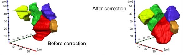
Cluster of WC grains taken from a large dataset 200um x 200um x 40um , which shows the 3D EBSD stacked data before and after the distortion corrections.

Keywords

BIB-SEM, FIB, 3D EBSD, distortion correction, serial section tomography

References

[1]          G. Nolze, Image distortions in SEM and their influences on EBSD measurements, Ultramicroscopy. 107 (2007) 172–183. https://doi.org/10.1016/j.ultramic.2006.07.003.

[2]          D. Rowenhorst, Removing Imaging Distortions Through Automatic Stitching of EBSD Mosaics, Microsc. Microanal. 19 (2013). https://doi.org/10.1017/s1431927613006193.

[3]          B. Winiarski, A. Gholinia, K. Mingard, M. Gee, G.E. Thompson, P.J. Withers, Broad ion beam serial section tomography, Ultramicroscopy. (2017). https://doi.org/10.1016/j.ultramic.2016.10.014.

[4]          G. Azzopardi, N. Azzopardi, Trainable COSFIRE Filters for Keypoint Detection and Pattern Recognition, IEEE Trans. Pattern Anal. Mach. Intell. 35 (2013) 490–503. https://doi.org/10.1109/TPAMI.2012.106.

[5]          S. Schaefer, T. McPhail, J. Warren, Image deformation using moving least squares, ACM Trans. Graph. 25 (2006) 533. https://doi.org/10.1145/1141911.1141920.

[6]          B. Winiarski, A. Gholinia, K. Mingard, M. Gee, G.E. Thompson, P.J. Withers, Correction of artefacts associated with large area EBSD, submitted to Ultramicroscopy 2021.


14:57 - 15:09

189 Measuring distortions in tetragonal tungsten bronze oxides using electron diffraction

Prof Richard Beanland1, Ms Chloe Ayers1, Mr Rhys de Gruchy1, Mr Thomas Brown2, Dr Andy Brown2, Prof. Steven Milne2
1University of Warwick, Coventry, United Kingdom. 2University of Leeds, Leeds, United Kingdom

Abstract Text

Tetragonal tungsten bronze oxides (TTBs) have promise as new Pb- and Bi-free Class-II dielectrics.  In particular, Sr2-2zCazYzNaNb5-zZrzO15, SNN, has a high Curie point (Tc~ 300°C), high εr(max) and second dielectric anomaly (T1 at <0°C) that increases the dielectric constant at low temperatures.  These properties make it one of the few materials capable of covering the -55°C to 300°C range required for the next generation of power electronics, which will play a crucial role in the impending energy transition from fossil fuels to electrification.

Uncaptioned visual

Fig. 1. The nominal TTB structure viewed along [001].

The structure of TTBs is complex, with perovskite-like blocks of corner-sharing NbO6 octahedra and cations A1 = Sr and A2 = Na (Fig. 1).  The prototype structure is tetragonal, but it exhibits distortions such as oxygen octahedral tilting that reduce symmetry and induce ferroelectricity.  These can be seen in diffraction patterns as superstructure spots.  An example is shown in Fig. 2, in which all the weak centring spots with Miller indices nn0, where n is an odd integer, arise due to structural distortions.

Uncaptioned visual

Fig. 2.  High dynamic range selected area electron diffraction pattern from [001] Sr2-2zCazYzNaNb5-zZrzO15


Using high dynamic range electron diffraction, the intensity of these spots can be measured quantitatively as a function of temperature.  Since they account for a very small amount (typically less than 1 millionth) of scattered intensity they can be described using kinematic diffraction theory and linked directly to distortion modes/order parameters of the material.


Keywords

High dynamic range imaging

Electron diffraction

Tetragonal tungsten bronze oxides


15:09 - 15:21

131 A new sample preparation workflow in the FIB-SEM for rapid, in-situ TKD analyses

Dr Pat Trimby, Dr John Lindsay
Oxford Instruments Nanoanalysis, High Wycombe, United Kingdom

Abstract Text

Since its development approximately 10 years ago, the transmission Kikuchi diffraction (TKD) technique has made the analysis of nanostructured materials in the scanning electron microscope (SEM) a relatively routine task, requiring only a conventional electron backscatter diffraction (EBSD) system. TKD has been successfully applied to a wide range of materials and application fields, ranging from heavily deformed alloys to sub-micrometre inclusions in meteorites (e.g. [1]). However, one of the main drawbacks of the technique is the requirement for an electron transparent sample, necessitating the same complex preparation steps as for any transmission electron microscope (TEM) experiment, such as dimple grinding, electropolishing, ion polishing or sample lift-out using a focused ion beam (FIB) SEM.

Here we present details of a new workflow for in-situ TKD sample preparation and analysis in a FIB-SEM. Unlike conventional approaches, this technique does not require any sample lift-out and the TKD analysis can follow on directly from the milling step, ideally without transfer to another SEM. The technique benefits from an EBSD-ready top surface, which can be achieved using conventional bulk sample preparation techniques or can utilise a pristine, as-deposited surface layer such as is typical in thin films. Initial analyses of the surface of interest can be carried out at 0° tilt or in the standard geometry for EBSD (see figure 1, steps 1 and 2) prior to the sample preparation. The preparation technique involves milling of a sloping trench on the side of the sample (figure 1, step 3) until electron transparency is achieved, and then a small additional tilt is required to bring the sample into the ideal orientation for off-axis TKD (figure 1, step 4). The big advantage of this technique is that the sample can be any thickness – unlike in-situ preparation techniques aimed at subsequent TEM analyses, in which the whole sample thickness needs to be milled (e.g. [2]) – and therefore the whole process can be completed in just a few minutes using a conventional Ga FIB SEM. The latest generation of plasma FIBs and femtosecond laser systems are ideal for this technique, significantly speeding up the process as well as opening up the additional potential of routine preparation of large areas (i.e. > 100 um field of view) for TKD analysis.

In this presentation we will show application examples using this preparation workflow, for both nanostructured and heavily deformed samples, and will discuss the future potential of the technique for standard, rapid nanomaterials characterisation in the FIB-SEM.

Uncaptioned visual

Figure 1. Workflow steps for rapid TKD sample preparation. 1. Optional imaging and / or X-ray analysis of the surface of interest. 2. Optional conventional EBSD analysis. 3. Milling step with the surface of interest now facing downwards. A sloping trench is milled on the side of the bulk sample, with the thinned region milled down to the necessary electron transparency. 4. TKD analysis geometry – this can be carried out in the geometry used for step 3 or with the thinned sample area rotated to a lower tilt angle, as shown here.

Keywords

Nanomaterials

TKD

FIB

Sample preparation

EBSD

References

  1. G. Sneddon et al., Materials Science and Engineering R: Reports, 110 (2016), p. 1-122.
  2. K. J. O'Shea et al., Micron, 66 (2014) p. 9-15.

15:26 - 15:29

79 Electron diffraction studies of commensurately modulated structures in bismuth transition metal oxide

Mr Satyam Choudhury1, Mr Vishnumahanthy Mohan1, Mr Hriddhi Ghosh1, Mr Avnish Pal1, Dr. Manish Singh2, Prof. Rajiv Mandal1, Dr. Joysurya Basu1
1Department of Metallurgical Engineering, Indian Institute of Technology (BHU), Varanasi, India. 2Department of Materials Science & Engineering, University of Connecticut, Storrs, USA

Abstract Text

Bismuth transition metal oxides (Bi-M-O, M = Cr, Mn) are well known for their multiferroic properties. Understanding multiferroic properties is dependent on our ability to resolve structure as well as chemistry of the resulting phases during synthesis. One of the issues pertaining to structure in this system relates to nature of commensurate modulation. One of the primary motivations of this investigation will be to understand nature of commensurate modulation along various crystallographic directions. The tool utilised for this purpose will be electron diffraction and related contrast imaging.

Synthesis of Bi-Cr-O and Bi-Mn-O compounds was done through solid state as well as through wet chemical routes. Powders obtained by these routes were drop cast on to the lacy carbon grid and then the specimen was placed inside double tilt holder in FEI Technai G2 T20 Transmission Electron Microscope (TEM) operated at 200 KV, to carry out investigation by complementary electron diffraction experiments through systematic tilting. Simulations of stereograms were carried out through JEMS.

Selected area electron diffraction (SADP) patterns were acquired from an appropriate specimen volume by adjusting the aperture diameter to ~0.5micron. It is observed that the diffraction patterns display variation of intensities. Aligning the electron beam confirming to a zone we were able to acquire the diffraction pattern. It is observed there is a systematic change in intensity indicating presence of commensurate modulation. After getting clear signature of diffracted spot representing symmetry of basic and modulated unit we established orientation relationship between them by overlaying stereogram corresponding to both the units. The simulated stereogram assembly act as a model to identify set of overlapping poles corresponding to basic and modulated units, inspection along such axis enable us to acquire diffraction pattern with clear signature of basic and modulated units. Validity of the simulated model has been approximately verified by obtaining series of complementary diffraction patterns through tilting at different orientations. Additionally this enables us to determine the structure of the basic unit, the nature and extent of modulation along specific crystallographic directions in these compounds. Signature of lattice fringes corresponding to planes of commensurately modulated unit was captured at relatively lower magnification by diffraction contrast imaging. Inspection along zone axis of commensurately modulated unit enables us to acquire diffraction pattern containing signature of higher order Laue zones (HOLZ). As the lattice parameter along z axis is quite large, it is possible to capture several Laue zones simultaneously. Signature of micro twin and in-plane rotational twin boundaries had been observed through electron diffraction. Signature of commensurately modulated unit and basic unit has been obtained through convergent beam electron diffraction. The symmetry of basic and modulated unit has been analysed.

Precise alignment of electron beam is the key to reveal unique structural features associated with commensurately modulated Bi-Cr/Mn-O compounds through electron diffraction. Diffraction signature of modulated unit could be independently obtained with or without signature of basic unit along specific direction however, the signature of basic unit cannot be obtained exclusively.


Uncaptioned visual

Figure 1 - Systematic tilting of the particle as shown in the bright field (BF) image (a) at different angular values of α and β (in degree) were listed in the series of acquired diffraction patterns shown in fig. 1 (b) to (g). At a particular orientation we were able to acquire diffraction pattern where [011] Zone Axis (ZA) of basic unit is oriented parallel to [012]M ZA of modulated unit corresponding to commensurately modulated Bi10Cr2O21 compound. However, in rest of the SADP acquired off the zone axis the diffraction signature appears complex with inhomogeneous distribution of diffracted intensities.

Keywords

Electron diffraction, Commensurate modulation, Crystallography, Stereogram

References

[1] Hill et al., J. Phys. Chem. B, vol. 106, no. 13, pp. 3383–3388, 2002.

[2] Grins et al., J. Solid State Chem., vol. 163, no. 1, pp. 144–150, 2002.

[3] D. B. Williams and C. B. Carter, Transmission Electron Microscopy, vol. 5, no. 721. 2009.

[4] The authors would like to acknowledge the financial support from UGC-DAE-CSR by the  award number CSR-KN/CRS-94/2017-18/282.

[5] The author would like to acknowledge the support from Department of Science & Technology inspired FIST programme. 


15:29 - 15:32

340 Comparative analysis of continuous rotation electron diffraction (cRED) data using Bloch-wave simulations.

Mr Anton Cleverley, Mr Yani Carter, Mr William Roberts, Professor Richard Beanland
University of Warwick, Coventry, United Kingdom

Abstract Text

Structure solution using electron diffraction (ED) has growing popularity over the past decade [1] and advances in computer control, detector technology and methodology now makes ED of nanoscale crystals widely accessible [2].  While structural refinement is possible using ED data, and structural parameters can have accuracy approaching that of solutions obtained from neutron or X-ray data [3], the match between calculated and measured intensities is invariably much poorer, manifesting as high R-factors [4].   The origin of this problem is still under investigation, but it has long been appreciated that the advantage of strong electron scattering, which allows nanoscale crystals to be analysed, also results in multiple scattering and dynamical diffraction. Attempts to minimise these effects, e.g. by using precession ED [5to average intensities, improves matters but does not eliminate the problem. 

 In convergent beam diffraction, good agreement between dynamically diffracted intensities and experimental data is possible and refinements of crystal structure using full dynamical calculations can give atomic coordinates to a precision of 0.2pm [6].  This suggests that high R-factors are not inevitable in ED data Here, we use Bloch-wave simulations of convergent beam electron diffraction using the program felix  [7] running on a cluster of >100 cores to model dynamical diffraction effects in continuous rotation ED (cRED) data ancompare it with experimental cRED datfrom a silicon crystal in the form of a [110] lamella approximately 80 nm in thickness.  

Experimental data was obtaineusing selected area diffraction on a JEOL 2100 LaB6 transmission electron microscope operating at 200 kV using a Gatan OneView camera running at 75 frames/sec over a 140° range, capturing ~1400 selected area ED (SAED) patterns in <20 seconds producing data up to ~4 reciprocal Ångstroms.  The resulting images were then processed using PETS2.0 [8] as a data reduction tool, giving integrated intensities suitable for crystal structure solution. Figure 1 shows a typical experimental SAED pattern (left) and the simulated peak positions determined using PETS2.0 (right).  Comparison of integrated experimental intensities I(meas) with calculated kinematical intensities Fhkl.Fhkl*, where Fhkl is the structure factor for reflection hkl and * indicates complex conjugate, show aessentially monotonic but non-linear dependency (Fig. 2). 

The PETS2.0 output was used to generate inputs to felix, giving complex amplitudes and intensities for crystals of the correct orientation and a range of thicknessesWe investigate the effects of varying sample thicknessspatial coherence and convergence angle on the expected intensities and optimise the fit between simulation and experiment using a full dynamical calculation.   


Uncaptioned visual

 Figure 1.  Left: typical SAED pattern from a silicon sample in the cRED data set.  Right: simulated PETS2.0 pattern showing Bragg reflections.   

Uncaptioned visual

Figure 2.  Comparison of measured integrated intensities I(meas) and calculated kinematical intensities Fhkl.Fhkl* for the silicon data in Fig. 1 

Keywords

Electron Diffraction
Structure Solution
Bloch-Wave Simulation
Silicon
PETS2.0
Felix
Jana2020

References

[1] Midgley, P. A. & Eggeman, A. S. (2015). IUCrJ 2, 126–136;  

[2] Mugnaioli, E. (2015). Acta Cryst. B 71, 737–739.  

[3] Wolff, A. M., et al. (2020). IUCrJ 7, 306–323.  

[4] Grimes, J. M., et al. (2018). Acta Cryst. D 74, 152–166.  

[5] Vincent, R. & Midgley, P. A. (1994). Ultramicroscopy 53, 271–282.  

[6] Hubert, A. J. M. et al. (2019) Ultramicroscopy 198, 1-9; Beanland, R., et al. (2021). Acta Cryst. A 77, 1–12.  

[7] Beanland, R., Evans, K., Ro¨ mer, R. A. & Hubert, A. J. M. (2019). Felix: Bloch wave method diffraction pattern simulation software. https://github.com/RudoRoemer/Felix. 

[8Palatinus, L. et al. (2019) Acta Cryst. B 75, 512-522. 

[9Petricek, V., Dusek, M., Palatinus, L. (2020). JANA2020 Crystallographic Computing System. Institute of Physics of the Czech Academy of Sciences, Prague, Czechoslovakia.


15:32 - 15:35

144 Unraveling dynamical behaviour of intergranular glassy films in Si3N4 ceramics during in-situ heating: exit wave reconstruction insights

Mr. Chiranjit Roy, Mr. Pritam Banerjee, Dr. Somnath Bhattacharyya
Department of Metallurgical and Materials Engineering, Indian Institute of Technology Madras, Chennai 600036, Chennai, India

Abstract Text

Dynamical behaviour of intergranular glassy films (IGFs) in undoped and Lu2O3- MgO doped Si3N4 ceramics was studied by using In-situ Transmission Electron Microscope (TEM) techniques. The experiment was performed with a Zeiss-912 (LaB6, Köhler illumination) TEM, heated from room temperature to 950°C, operated at 120 KeV and equipped with an in-column energy filter (Carl Zeiss AG, Germany). Exit wave reconstruction with a set of focal series images at different temperatures was used to get more insights into IGFs. Mean full-width half maximum (FWHM) of phase changes across the IGFs and mean phase difference between adjacent Si3N4 grains and IGFs were used to study the variation during in-situ heating in case of both undoped as well as doped samples. It is shown in the results that in the case of undoped samples, IGFs maintain equilibrium configuration. In contrast, the doped one exhibits some deviation during in-situ heating, which indicates that the mean inner potential has some contribution during heating [1]. Mean inner potential differences between IGFs and adjacent grain of doped sample at room temperature exhibit higher value than that of the undoped one due to rare earth element segregation [2] within IGF which is possibly the cause of the difference in the dynamical behaviour of IGFs observed in the present study.

Keywords

Exit wave reconstruction, in-situ heating, TEM, intergranular glassy film, Si3N4

References

[1]      S. Bhattacharyya, C.T. Koch, M. Rühle, Projected potential profiles across interfaces obtained by reconstructing the exit face wave function from through focal series, Ultramicroscopy. 106 (2006) 525–538.


[2]        Y. Jiang, S.H. Garofalini, Effect of thickness and composition on the structure and ordering in La-doped intergranular films between Si3N4 crystals, Acta Mater. 59 (2011) 5368–5377.


15:40 - 16:10

4 Designing Novel Functional Materials Through Data-Infused Microscopy

Dr. Steven Spurgeon
Pacific Northwest National Laboratory, Richland, USA

Abstract Text

The development of advanced nanomaterials synthesis techniques over the past several decades has sparked a renaissance in the design of clean energy and quantum computing technologies. While it is now possible to produce nanostructured materials in almost limitless configurations, engineering of desirable functionality for device applications depends on precise control of atomistic structure and defects. We have developed a materials design strategy using data-infused scanning transmission electron microscopy to richly inform synthesis and modeling efforts. Here I will describe our efforts toward a new data-centric approach that is redefining how we study materials and enabling us to extract truly statistical information at scale. I will illustrate how vast, multi-modal data streams from modern electron microscopy can help unlock the promising materials of the future.

Keywords

scanning transmission electron microscopy, data science, machine learning, nanomaterials, synthesis