10:00 - 10:30
Thermoelectric generators (TEGs) convert heat into electrical power and their robust, reliable power generation underpins their deployment in the Mars rovers. A more down-to-Earth application is to scavenge waste thermal energy from energy-intensive industries including glass, steel and cement manufacture. These currently account for ~15% of global CO2 emissions, so improving their energy efficiency could make a significant contribution to efforts to reduce climate change.
Half-Heusler alloys (hHAs) are a family of intermetallic compounds that have become leading contenders for mass production and commercialisation of TEGs: they are stable, mechanically robust and employ abundant, inexpensive elements. However, they are also compromised by relatively low thermoelectric performance. Almost all research has focused on optimising hHAs through the twin strategies of (i) electronic doping via atomic substitutions and (ii) enhanced phonon scattering by introducing structures on the nanometre length-scale. Nevertheless, the predicted performance is usually degraded by electron and phonon scattering arising from structural features with micrometre, if not millimetre dimensions. Here, I outline a comprehensive suite of microscopies in order to develop a multi-lengthscale appreciation of the links between materials structure and ultimate TEG performance.
I will focus on structural characterisation of the most promising TiNiSn and related Heusler alloys. Elemental mapping by energy dispersive x-ray analysis [1] revealed remarkably inhomogeneous structuring, phase-segregation effects and grain-by-grain, micron-scale variations [2]. Dopants will be shown to improve the structural homogeneity and Cu is found to be an effective electronic dopant. It has surprisingly low solubility in the bulk material, with excess being extruded to grain boundaries. On the atomic scale, a combination of scanning transmission electron microscopy, electron energy loss spectroscopy and atom probe tomography was used to identify two main types of grain boundary. In the first type, Cu forms ‘wetting layers’ that facilitate coherent grain boundary formation [2]. In the second type, Cu acts as a surfactant, drawing impurities (notably oxides) out of the bulk [3,4]. Both grain boundary complexions will influence TEG performance.
I will then turn to thin film studies, using pulsed laser deposition to deposit epitaxial thin TiNiSn films that act as model systems for studies of phase segregation [5,6]. The ideal deposition conditions will be discussed; absolute quantification of the stoichiometry using electron energy loss spectroscopy will be outlined [7]; and annealing experiments in-situ to the electron microscope will be shown to reveal novel aspects of phase segregation and spontaneous nanostructuring. A unique combination of the Quantum Detectors MediPix direct electron counting detector and NanoMegas DigiStar precession electron diffraction system was used for rapid, high-fidelity acquisition of pseudo-kinematical electron diffraction patterns with high dynamic range. The resulting structural assessment was then correlated with EELS measurements in a form of correlative spectrum imaging. We derive a non-linear relationship between lattice parameters and composition, and find a preference for doped hHAs to segregate into ‘full’ and ‘half’ Heusler alloy phases.
My main theme is that no one microscopy technique is sufficient for full structural characterisation of bulk materials; but that with multiple techniques spanning multiple length-scales, much progress can be made towards viable devices.
ACKNOWLEDGEMENTS
This work was conducted through collaboration with Dr. RWH Webster, Dr. JE Halpin (University of Glasgow), Dr Paul Bagot (University of Oxford) and Dr. J-WG Bos (Heriot-Watt University). It was funded principally by the EPSRC through grants EPSRC grants EP/N017218/1 and EP/P001483/1.
thermoelectrics, Heusler alloys, nanocharacterisation, electron spectrocopy, atom probe tomography, correlative microscopy
10:30 - 10:42
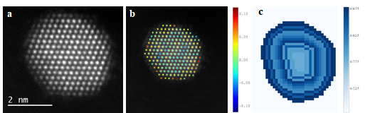
Heusler alloy of Co2FeSi (CFS) has been regarded as one of the most promising candidates for spintronics applications due to its high magnetic moment and theoretically possible full spin polarization1,2. These desired properties are heavily affected by the presence of structural ordering of phases within CFS. In this study, phase ordering of CFS full-Heusler thin films were investigated using correlated EDS and 4D-STEM approaches. Unsupervised machine learning (ML) methods including decomposition and clustering approaches3 were implemented to provide insight into the structural and solute variations within the films. Previous XRD measurements suggested B2 (Pm-3m) and L21 (Fm-3m) ordering, however, PCA and fuzzy clustering ML methods indicated an unexpected phase in addition to B2 and L21. This minority superstructure may help to explain variations in magnetocrystalline anisotropy in these films. Correlated EDS signals provide a pathway to identify the unexpected phase. Figure 1 shows PCA and fuzzy clustering outputs of a CFS thin film grown on Si(111). Figure 1-a belongs to B2/L21 phase, evident by the (200) (red circle) and (111) type reflections, and Figure 1-b belongs to the unexpected phase of this system.
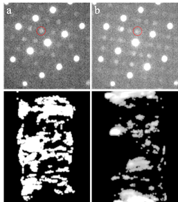
Figure 1. Decomposed diffraction patterns and accompanying memberships maps of two distinct ordered phases of CFS thin film.
Cluster memberships (the lower panels) show how these phases are complementary in the films, similar studies on composition variation in the films are underway to address the possibility of local segregation of solute causing these differences in superstructure ordering.
Heusler alloys, 4DSTEM, machine learning
1. Gercsi, Z. et al. Spin polarization of Co 2FeSi full-heusler alloy and tunneling magnetoresistance of its magnetic tunneling junctions. Appl. Phys. Lett. 89, 082512 (2006).
2. Zhu, W. et al. Magnetization precession and damping in Co 2 FeSi Heusler alloy thin films. J. Magn. Magn. Mater. 479, 179–184 (2019).
3. Martineau, B. H., Johnstone, D. N., van Helvoort, A. T. J., Midgley, P. A. & Eggeman, A. S. Unsupervised machine learning applied to scanning precession electron diffraction data. Adv. Struct. Chem. Imaging 5, 3 (2019).
10:42 - 10:54
Summary
Xe-PFIB equipped with a high speed EBSD camera was used to carry out three-dimensional electron backscatter diffraction (3D EBSD) on a thin film CdTe solar cell with a graded CdSeTe (CST layer) layer at the front of the device. A chunk lift-out of volume 40x50x4µm with slice thickness of 50nm was analysed. Data extracted includes grain size, texture, and coincident site lattice (CSL) change as a function of depth. The (111) intensity and grain size decreases when the slicing approaches from CdTe at the back to the CST layer at the front. The CST layer has mostly randomised texture but with a comparatively minor preference in (001) intensity. The CST boundary data shows a 15% reduction in the frequency of Σ3 grain boundaries relative to the CdTe layer.
Introduction
Thin film CdTe photovoltaic devices are the most successful second-generation solar technology. By being a direct band gap semi-conductor, only 2µm of absorber layer is needed to absorb majority of the incident sunlight, providing a natural cost advantage over crystalline Silicon. The efficiency of thin film CdTe devices has recently increased to 22.1% by the addition of the CdSeTe and by substituting the CdS n-type layer with a wide band gap metal oxide [1]. However, the efficiency is still well short of the theoretical conversion efficiency limits of ~ 30%[2] due to inefficient passivation of defects at interfaces and grain boundaries[3].
High-speed 3D EBSD has been used to measure microstructural changes of CdSeTe/ CdTe devices as a function of depth. The novel Xe-PFIB with high speed EBSD acquisition enables the study of high efficiency thin film solar cells in 3D to enhance the understanding of the microstructural evolution. This allows correlations between the microstructure and device efficiency.
Experimental
The CdSeTe/CdTe device structure consists of TEC 10 glass superstrate with a 100nm sputtered MgZnO (MZO) buffer layer. A~ 800nm thick layer of CdSeTe is deposited on the buffer followed by ~2.5µm of CdTe. Full device fabrication details have been reported elsewhere[4].The CdCl2 treatment has been applied to the device which allows for Chlorine to passivate grain boundaries and significantly to enhance performance.
A Helios G4 Xe PFIB equipped Oxford Symmetry CMOS detector was used for sample preparation and scanning. An in-plane chunk lift-out procedure was performed to lift part of the device and attach it to a silicon wafer edge to reduce shadowing effects. A chunk size of 40x50x4µm was used with fixed accelerating voltage of 10kV, 6.4nA and a pixel dwell time of 0.64 ms. Chunk lift-out step used 60nA ion beam current.
Milling and scanning procedures were automated, and each cycle of milling and scanning took approximately 20 minutes. PFIB milling rate in general can be in order of 10x faster than convent Ga-FIB milling rates. Fiducial markers were used to maintain the milling in a constant position. For comparison, a 2D cross section was also produced to compare with the 3D rendered microstructure. Standard Aztec, hkl Channel 5 software was used to analyse individual 2D slices. Data such as inverse pole figures and direct numerical value of texture intensity in the normal direction was extracted. The rendered voxel 3D structure was produced by processing the slices in Dream 3D [5] and visualised in Paraview software [6].
Results and Discussion
Fig. 1 is a cross section through the device showing the indexed layers. The cross section provides a useful indication of the accurate of the milling step size. 3D slicing was performed on the plane view. The initial surface roughness is random so not every slice was usable to extract useful data.
Each 2D slices was analysed with a focus on extracting grain size variation, texture evolution and the concentration of S3 boundaries. The average grain size variation as a function of depth was determined with 65 slices. Grain size remains mostly constant about 2.5±1 mm in the CdTe region until the transition to the CdSeTe layer. The grain size in the CdSeTe region of the device was ~ 1.7±0.8mm.
The intensity of the (111) texture remains constant in the CdTe layer. However, the intensity of the (111) texture varies by about 80% when transitioning to the CdSeTe layer due to the change in crystal structure. S3 CSL boundaries that are the most common type observed in CdTe devices. Their occurrence was quantified, and this is shown in Fig. 2. The CdTe region contains a higher frequency of S3 boundaries compared to CdSeTe (35% vs 20%).
Fig. 3 and 4 show the 3D reconstruction. The main problem when carrying out 3D analyses with these devices is charging and drifting, which can distort the microstructure. Fig 3 shows the IPF (Z axis) and Fig.4 shows a skeletal grain boundary reconstruction with S3 boundaries highlighted in red. The current 3D reconstruction maps do not show any direct evidence of any tilt and twist angles relation to the neighbouring grains. Further work will be required to corelate the tilt and twist boundaries with the effect of Chlorine used in device activation to these boundaries. It is crucial to understand the 3D geometry of the GBs to enable GB engineering of the CdTe and CdSeTe in the device.
Conclusions
3D EBSD has enabled the study of the microstructural evolution through the thin film thickness of a high efficiency CdSeTe/CdTe device. The grain size remains unchanged at ~ 2.5 µm in the purely CdTe region and then reduces to~1.7 µm in CdSeTe layer at the front of the device. The (111) texture in the CdTe layer changes to a more random texture with a slight increase in (100) in the CdSeTe layer. The 3D dataset also revealed a 15% decrease in S3 boundary occurrence in the CdSeTe layer.
3D-EBSD, grain size, texture, depth, CdTe, CST
[1] J. Major, “Grain boundaries in CdTe thin film solar cells: a review,” Semicond. Sci. Technol., vol. 31, no. 9, p. 93001, 2016
[2] W. Shockley and H. J. Queisser, “Detailed balance limit of efficiency of p-n junction solar cells,” J. Appl. Phys., vol. 32, no. 3, pp. 510–519, 1961.
[3] D. Kuciauskas, J. Moseley, P. Ščajev, and D. Albin, “Radiative Efficiency and Charge-Carrier Lifetimes and Diffusion Length in Polycrystalline CdSeTe Heterostructures,” Phys. Status Solidi - Rapid Res. Lett., vol. 14, no. 3, pp. 1–6, 2020.
[4] T. Shimpi et al., “Influence of Process Parameters and Absorber Thickness on Efficiency of Polycrystalline CdSeTe/CdTe Thin Film Solar Cells,” in 2020 47th IEEE Photovoltaic Specialists Conference (PVSC), pp. 1933–1935, 2020.
[5] M. A. Groeber and M. A. Jackson, “DREAM.3D: A Digital Representation Environment for the Analysis of Microstructure in 3D,” Integr. Mater. Manuf. Innov., vol. 3, no. 1, p. 5, 2014.
[6] U. Ayachit, The ParaView Guide: A Parallel Visualization Application. USA: Kitware, Inc., 2015.
10:54 - 11:06
Ferroelectrics are polar materials which form domains in order to minimize its depolarization field. However, under particular boundary conditions these materials can exhibit domain topologies that mirror the ones found in magnets, even polar vortices. The important difference between the magnetic and ferroelectric domains is that the latter one significantly distorts the crystal lattice. In particular, it enables the use of dark field transmission electron microscopy (DF-TEM), which shows diffraction contrast between regions where the polarization is oriented along different directions.
Here, we study epitaxially grown single layers of PbTiO3 (PTO) sandwiched between two SrRuO3 (SRO) electrodes on SrTiO3 (STO) buffered DyScO3 (110)o substrate. The local structure is resolved using a combination of scanning transmission electron microscopy (STEM) and DF-TEM. While SRO is a metallic electrode which should stabilize the polarization, cross-sectional STEM reveals pairs of clockwise/anti-clockwise formed in the ferroelectric layer (Figure 1a, b). Furthermore, plan view DF-TEM imaging shows an extended polar texture, which is presented as two periodicities along the principal [h00] and [0k0] axes, resulting in a labyrinth-like domain topology (Figure 2a). High-Dynamic-Range (HDR) electron diffraction reveals incommensurate satellites decorating the film diffraction spots (Figure 2b, c), with a distribution along the principal axes to match the X-ray data. Further analysis of the plan-view data shows the two periodicities are interwoven in such way that no region within the ferroelectric layers shows uniform domains, mimicking the recently discovered incommensurate spin crystal found in magnets. Finally, we propose a model which agrees with the experimental observations.
Figure 1 | Cross-sectional STEM. a, Annular Dark Field STEM (ADF-STEM) of the SRO/PTO/SRO tri-layers. b, Unit cell polarization mapping of the ADF-STEM image revealing the formation of clockwise and anti-clockwise vortices within the PTO layer. The scale bar is 2nm. |
Figure 2 | Planar view DF-TEM. a, DF-TEM under two beam condition reveals the domain topology. b, Recorded HDR electron diffraction showing the illumination conditions. c, The diffraction spots corresponding to the PTO layer are decorated with incommensurate satellites, evidence of the domain structure. |
11:11 - 11:14
Semiconductor nanowires are favoured in many optoelectronic applications over thin films due to their geometry, which facilitates a large surface area at a lower footprint, lower material consumption and low defect densities. The defect elimination capability of nanowires stems from the availability of a free surface within close proximity that attracts defects with strain fields, such as dislocations. III-V compound semiconductor nanowires are typically grown in <111>B direction and despite the absence of such defects, the planar twins that easily form perpendicular to this growth direction have long debilitated the field (Figure 1 (a)). Although they do not form non-radiative recombination centres, twin planes disrupt carrier propagation and induce changes in the band structure [1]. Recently, there has been much interest to eliminate these twin planes by growing nanowires in alternative orientations such as [100] and <111> A [2-4], by using the precursor pre-flow technique[2,3] to induce vertical nucleation.
Nanowire grown along these directions were long believed to be twin-free due to their inherent incapability to form twins; namely, the twin-forming {111} planes being inclined to the nanowire-catalyst interface in [100] nanowires and centre nucleation in <111> A nanowires. Even though twins that form perpendicular to the growth direction are absent, it is seen that inclined twins may still form in these nanowires, with their densities depending on the growth parameters (Figure 1 (b)). These inclined twins were also believed to be semi-benign in nature, like those that form perpendicular to the growth in <111> B nanowires.
Using InP [100] and GaAs <111>A nanowires as model systems, this work demonstrates that the inclined twins can terminate within the nanowire, forming non-radiative defects with far more detrimental effects than those perpendicular to the growth direction in <111> B nanowires. Atomic resolution scanning transmission electron microscopy (STEM) and dark field TEM analysis supported by multi-slice STEM simulations reveal different configurations of the inclined twin termination within the two types of nanowires. As a result of twin termination, defects with straight <110> line direction, are formed in <111> A nanowires (Figure 1 (c)), whilst loops with changing line direction and kinks are formed in [100] nanowires as shown in Figure 1 (d). The latter also explains the blurriness in the twin termination core of [100] nanowires (Figure 1 (e)). Micro-photoluminescence studies confirm the adverse effect of these defects on nanowires’ optical properties. Finally, defect-free nanowires are grown in both orientations by optimising the growth parameters.
Figure 1. (a) TEM image of a GaAs <111> B nanowire showing twin formation (red arrows) perpendicular with the growth direction. (b) InP [100] and GaAs <111> A nanowires showing inclined twins. Inclined twins that terminate within the nanowire are marked with blue arrows. (c) ADF STEM image taken along <110> zone axis showing the clear defect core in a GaAs <111> A nanowire’s terminating twin and the inset schematic shows the straight <110> defect line on the corresponding {111} plane in a tilted view. (d) Schematic and a dark field image showing the kinked loop nature of the twin termination line in [100] nanowires. (e) BF STEM image showing the lack of a clearly visible defect core in [100] nanowires.
[1] J. Bao. et.al., Nano Letters 2008, 8 (3), 836-841.
[2] J. Wang et.al., Nano Letters 2013, 13 (8), 3802-3806.
[3] X. Yuan et.al., Advanced Materials 2015, 27 (40), 6096-6103.
[4] H. A. Fonseka et.al., Nanoscale Research Letters 2019, 14, 399.
nanowires, defects, III-V compound semiconductors, nanomaterials, twin defects, multi-slice simulations, 1D structures
[1] J. Bao. et.al., Nano Letters 2008, 8 (3), 836-841.
[2] J. Wang et.al., Nano Letters 2013, 13 (8), 3802-3806.
[3] X. Yuan et.al., Advanced Materials 2015, 27 (40), 6096-6103.
[4] H. A. Fonseka et.al., Nanoscale Research Letters 2019, 14, 399.
11:14 - 11:17
In this work, we present a novel methodology to precisely measure strain distribution on atomic resolution annular dark-field (ADF) images of the bimetallic (Pt/Co) nanoparticles. Electron energy loss spectrum (EELS) and energy dispersive X-ray (EDS) signals are recorded simultaneously to analyse the composition distribution of the Pt/Co nanoparticles. Subsequently, the composition variations, size and strain distributions of the Pt/Co nanoparticles are related to their enhanced catalytic activities.
Fuel cells are very promising energy-conversion devices due to their high efficiency and near-zero carbon emission footprint. Fuel cells still require a high mass of precious metal Pt as an electrocatalyst to ensure sufficient power output efficiency, but the sources and cost of Pt greatly limit its commercial application in fuel cells technology. Thus, the development of high-active and low-cost electrocatalysts is of much significance for the commercialization of fuel cells. Compared with Pt, bimetallic catalyst nanoparticles (Pt/Co) exhibit excellent performance with less mass of precious metal, but the intrinsic mechanism of this enhanced catalytic performance has not been fully explained. The properties of nanoparticles mainly depend on size, structure, morphology, and composition. Previous work has found that the finite size, domain structure, and composition variations can introduce strain to nanoparticles[1]. The strain has also been shown to be related to the catalytic activity of nanoparticles through density functional theory calculations[2]. Being able to measure the local composition and to relate composition variations to the strain within nanoparticles will further our understanding of the operation of heterogeneous catalysts.
Our proposed global strain minimization algorithm is based on the detection of atom columns on atomic resolution images in real space. A reference grid is generated and refined from a selected area of the nanoparticle. The atomic site-specific strain map is obtained by derivating the discrete displacement fields. A large ensemble of the on-axis Pt/Co nanoparticles with different sizes are imaged and strain-measured to relate strain to the finite size and particle shape. Atomic resolution ADF images, EDS and EELS spectrum images are acquired simultaneously. The experimental spectroscopic partial scattering cross-sections of a single atom are calibrated using needle and nanoparticle standards. To obtain the quantitative composition distribution maps of the bimetallic nanoparticles, the number of Co atoms and Pt atoms are calculated from the EELS and EDS signals, respectively. The composition variations are subsequently related to strain.
To achieve high resolution of STEM imaging, the JEOL ARM-200F electron microscope fitted with a probe-forming aberration corrector was used to acquire the ADF image of the on-axis Pt/Co nanoparticle, Figure 1a. Strain analysis was performed on this nanoparticle, Figure 1b showing the distribution map of lattice areal expansion (εxx+εyy). The areal expansion map demonstrates that this bimetallic nanoparticle has strain restricted to a few outer layers. The spectroscopic signals are collected simultaneously on this nanoparticle. The composition distribution map obtained by quantifying these spectroscopic signals is shown in Figure 1(c). It indicates the Pt enrichment at the surface of this bimetallic nanoparticle.
Both the composition map and strain distribution map demonstrate the ‘core-shell’ effect of the bimetallic Pt/Co nanoparticle. The expansion of the local lattice parameter can be observed as the proportion of Pt atoms increases.
Figure 1 (a) The atomic resolution ADF image of a Pt/Co nanoparticle. (b) The normal strain (εxx+εyy) distribution map of the particle. (c) The percentage of Pt atoms in each shell from the surface to core of the particle.
Nanoparticle; STEM; Strain; EDS; EELS; Fuel Cell; Catalyst
1. Pingel, T.N., et al., Influence of atomic site-specific strain on catalytic activity of supported nanoparticles. Nature communications, 2018. 9(1): p. 1-9.
2. Gavartin, J., et al., Exploring Fuel Cell Cathode Materials: A High Throughput Calculation Approach. ECS Transactions, 2009. 25(1): p. 1335.
11:17 - 11:20
Ferroelectric materials have a myriad of applications such as in microelectromechanical systems (MEMS)1 and non-volatile random access memories2 due to their switchable electrical polarisation and piezoelectric properties. For such device applications, deterministic control of the intrinsic polarisation state of the ferroelectric thin film is of paramount importance since an initial defined monodomain state (where the polarisation is uniformly oriented) is often desirable. Realising an intrinsic, as-grown, monodomain state is therefore advantageous since it would eliminate preliminary poling steps which can be detrimental due to modification of the surface chemistry of the films.3 Key factors dictating the intrinsic polarisation states in epitaxial films include electrostatic boundary conditions and epitaxial strain which can be readily altered by, for example, the choice of bottom electrode and/or substrate,4,5 film thickness5 or changes to the chemical environment.6
Here, we report deterministic control of the intrinsic polarisation of epitaxial PbTiO3,7 a canonical ferroelectric that provides an ideal model system owing to its versatility, the wealth of literature available and its inclusion in the Pb(Zrx,Ti1-x)O3-based solid solutions which are widely employed in commercial devices.8 As a function of increasing growth temperature, we establish a transition from monodomain “up” through to polydomain and finally monodomain “down”. A combination of energy dispersive X-ray spectroscopy (EDX) and scanning transmission electron microscopy (STEM) reveals variations in stoichiometry and out-of-plane strain through the film thicknesses resulting in polarisation gradients which we directly visualise via atomic resolution STEM. These highly local observations are complemented by larger scale measurements by means of X-ray diffraction, Rutherford backscattering spectroscopy and piezoresponse force microscopy. The detailed characterisation presented here enables a comprehensive understanding of the origin of intrinsic polarisation states in these ferroelectric thin films. Moreover, adjustment of growth temperature provides a particularly simple method for control of polarisation, providing an additional tuning parameter for domain engineering and the potential realisation of more complex films with unusual polarisation textures such as vortex and skyrmion-like topologies.
Functional Semiconductor and Oxide Materials, Microscopy of Interfaces and Heterostructures, High Resolution Chemical and Structural Analysis
1 S. Trolier-Mckinstry and P. Muralt, J. Electroceramics 12, 7 (2004).
2 J.F. Scott and C.A. Paz De Araujo, Science 246, 1400 (1989).
3 N. Domingo, I. Gaponenko, K. Cordero-Edwards, N. Stucki, V. Pérez-Dieste, C. Escudero, E. Pach, A. Verdaguer, and P. Paruch, Nanoscale 11, 17920 (2019).
4 H. Lu, X. Liu, J.D. Burton, C.W. Bark, Y. Wang, Y. Zhang, D.J. Kim, A. Stamm, P. Lukashev, D.A. Felker, C.M. Folkman, P. Gao, M.S. Rzchowski, X.Q. Pan, C.B. Eom, E.Y. Tsymbal, and A. Gruverman, Adv. Mater. 24, 1209 (2012).
5 D.G. Schlom, L.-Q. Chen, C.-B. Eom, K.M. Rabe, S.K. Streiffer, and J.-M. Triscone, Annu. Rev. Mater. Res. 37, 589 (2007).
6 R. V. Wang, D.D. Fong, F. Jiang, M.J. Highland, P.H. Fuoss, C. Thompson, A.M. Kolpak, J.A. Eastman, S.K. Streiffer, A.M. Rappe, and G.B. Stephenson, Phys. Rev. Lett. 102, 047601 (2009).
7 C. Weymann, C. Lichtensteiger, S. Fernandez-Peña, A.B. Naden, L.R. Dedon, L.W. Martin, J. Triscone, and P. Paruch, Adv. Electron. Mater. 6, 2000852 (2020).
8 G.H. Haertling, J. Am. Ceram. Soc. 82, 797 (1999).
11:25 - 11:37
Ceria is one of the most studied nanomaterials with applications across catalysis, biomedics, energy storage and environmental protection. This versatility is owed to its high redox activity and structural stability. Novel structures are constantly being developed aiming for improved catalytic performance. Rod-shaped nanoparticles are of particular interest, as they present higher activity than other ceria nanostructures of similar surface area. This is attributed to the presence of exposed planes and to the number of {100} and {110} surfaces. More recently, the engineering of structural defects in nanorods has shown potential for improved catalytic activity and increase in the concentration of reaction centres. Our work presents, for the first time, a three-dimensional electron tomography characterisation of the shape and distribution of novel large meso-pores in ceria using a modified algorithm of geometric tomography as a reliable tool for reconstructing defective and strain-affected nanoobjects. Most pores are confirmed as “negative-particle” or “inverse-particle” cub-octahedral shapes located exclusively beneath the flat surface of the rods separated via a sub-5 nm thin ceria wall from the outside. Lattice fringe analysis by HRTEM can resolve the orientation relationship between lattice planes, pore surfaces, and rod surfaces. New findings also comprise elongated “negative-rod” defects, seen as embryonic steps towards nanotubes.
Electron tomography; 3DTEM; Ceria; Nanorods; Mesoporous materials; Catalytic materials
11:37 - 11:49
Aluminium alloys are widely used in aerospace and aeronautic industries because of their excellent strength-to-weight ratio. In these applications, overloads can occur, damage the part and lead to its replacement. In order to increase the part’s lifetime, a solution would be to use a material able to heal its damage and restore its continuity. The most advanced man-made self-healing materials are polymers. They are composed of encapsulated healing agents which are released when a crack propagates, leading to the crack closure [1]. Designing self-healing metals is more challenging because the damage is usually healed via solid-state diffusion, which cannot be triggered at room temperature. It requires a heat treatment to trigger the migration of the healing agents and allow the healing of these cracks and/or cavities [2]. However, the damage and its healing are hard to quantify using only surface observations. Additionally, due to a multiscale distribution of the microstructure and damage size, a multiresolution and multimodal imaging approach with a spatial resolution from micro- to nano- scale is required to evidence the microstructure healing efficiency. Correlative tomography (CMT) [3] is a concept/workflow of spatial registration in two and three dimensions (2D and 3D) of many imaging modalities - light microscopy (LM), electron/ion microscopy (EM, IM), X-Ray tomography, 2D/3D EBSD [2], EDS, Raman, etc.) - that allows various types of information, and at different length-scale, to be collected for the same region of interest (ROI).
Therefore, the aim of this research was to develop a robust and controlled multiscale analysis protocol for evaluation of the cracks and pores dimensions within a healable AlMg alloy, using three-dimensional (3D) correlative microscopy/tomography. In this contribution, we utilized a non-destructive character of X-ray based imaging linked with high-resolution 3D volume analysis within PFIB-SEM via advanced correlative data acquisition and processing platform, available within Avizo software (Themo Fisher Scientific) [4].
Laser powder bed fusion (L-PBF) also called Selective laser melting (SLM) was used to manufacture a healable aluminium alloy. After the additive manufacturing process, the parts contained defects such as porosity and cracking. Therefore, a heat treatment was applied in order to restore the metallic continuity by melting the eutectic phase and its migration to these defects. Applied 3D data collection strategy required scanning, using µCT lab-based system (TESCAN XRE HR, Belgium) of a whole sample volume with voxel size of 2.5µm, in order to identify a sub-volume region for further investigation with higher resolution (0.6 µm voxel size) scan. Additionally, a pre-defined sample section has been investigated using TOMCAT beamline at Swiss Light Source SLS facility of Paul Scherrer Institute, providing high quality 3D data with 0.65 µm voxel size. After inspection of high resolution µCT data, a 100 µm3 volume region of interest (ROI) has been defined at a location indicating a characteristic defect. The specific ROI μCT data and sample surface SEM images have been co-registered in order to define the specific ROI coordinates within μCT images and trace it with the Plasma FIB-SEM via Maps-Avizo navigation and visualization software platform. Automated serial sectioning tomography (SST) has been performed at the specific sample location using the Xe Plasma FIB-SEM microscope (Themo Fisher Helios Hydra DualBeam, SST SEM back-scattered electron images with 60 nm voxel size) (Figure 1). Finally, data from FIB-SEM study were combined with μCT results using the visualization and quantification Avizo research platform. A critical defect type of a crack originating from the internal porosity has been traced with multi-resolution tomography approach (Figure 1) with precision of 5 µm. High quality synchrotron tomography results revealed presence of micro-pores in surrounding of the crack origin. μCT data guided applications of PFIB-SEM system in the workflow allowed in excess hundreds of microns size cross-sections in all dimensions, and SEM recording of nano- sized microstructural features at the identified ROI. The details of the L-PBF microstructural features efficiency have been evidenced thanks to post-tomography correlation with PFIB-SEM nano-scale 3D information. These preliminary results indicate that the correlative microscopy approach for acquisition of the serial multi-resolution tomography data correlated with FIB-SEM tomography allow for precise location and characterisation of the critical defects. Furthermore, investing as built sample with multiscale tomography approach followed by extended correlative imaging of the same location at the heat-treated sample can lead to better understanding and quantification of the healing mechanism.
Figure 1. Correlative microscopy approach used in the current study.
Correlative Tomography, L-PBF, aluminium, self-healing
[1] Ghosh, S. Wiley, 2009.
[2] Arseenko, M., et al. ICSHM, 2019.
[3] Burnett, TL., et al. Scientific Reports 4, 2014
[4] Winiarski, B., et al. Microsc. Microanal. 25 (Suppl 2), 2019
11:52 - 11:55
Ferroelectric materials are an integral part of a variety of smart devices, such as sensors and actuators, due to their unique properties that can be controlled by external fields (temperature, electric field and stress) [1]. The characteristic marker of a ferroelectric material is the formation of domains below a critical temperature (TC), where the utility is often derived from the ability to switch the polarization of the domains [2]. The phase transition results in several domain variants of the lower symmetry phase, which arrange into energetically favourable patterns, based on a complex interplay between the system’s spontaneous strain and polarisation.
Whilst ferroelectric switching behaviour under external fields has been extensively studied [3], the behaviour of domains under thermal response has been largely unexplored until recently. Most exciting, is the evidence of a structurally bridging low-symmetry phase that exists between the orthorhombic and tetragonal phases in seminal ferroelectrics such as BaTiO3 [4]. It has been found that such monoclinic phases can be stabilised by competing interactions in complex multidomain structures at thermotropic phase boundaries (TPBs) in bulk BaTiO3 [5, 6], with similar behaviour also reported in low strain BaTiO3 thin films [7-9]. This is a significant finding, because intermediate monoclinic phases are known to cause a high piezoelectric response at morphotropic phase boundaries (MPBs) [10]. To date, there has been little experimental work that explores how the internal interactions of multiple domains can induce this phenomenon, hence hindering the practical use of this high-performance phase [11].
This work focuses on thermally driven domains in thin film-like single crystal BaTiO3 lamellae. We use in-situ heating and scanning transmission electron microscopy (STEM) techniques to provide a unique insight into the physical phenomena of 90° domains at low temperatures (20°C - 50°C). We observe that <100>pc and <110>pc domain variants exist in metastable configurations at temperatures < 50°C, where the domain walls can deviate significantly from the symmetry-prescribed crystallographic planes, indicative of a low symmetry bridging phase (see Fig. 1). Given that these domains are 90° ferroelastic domains, nanobeam electron diffraction (NBED) was employed to map the local strain fields as a function of temperature, in order to gain insight into the local elastic competition between the domain variants (see Fig. 2). This revealed that a complex network of domain variants can induce a TPB-like behaviour in lamella single crystal, without the need for complex chemistry, lattice mismatch, shear stress or a transverse electric field. Thus, alluring to an alternative and powerful tool for property enhancement and domain engineering.
Fig. 1: In-situ heating STEM between 20°C - 50°C in a <100>pc BaTiO3 lamella (∼150 nm). At (a) 20°C, the domain walls lie along <100>pc (dashed green arrows), but can meander significantly from the fixed crystallographic plane. At (b) 35°C, there is direct competition between the <100>pc and <110>pc (yellow dashed lines) domain variants and there exists many in-between metastable domain configurations. By (c) 50°C, the walls lie almost exclusively along the <110>pc, with no deviation from the fixed crystallographic plane.
Fig. 2: NBED of a complex domain configuration in a BaTiO3 lamella at 20°C, using an EMPAD detector, low dose conditions and the <100>pc reflections. (a) Scan image from the EMPAD detector, (c-f) represents the c/a ratio maps in the εxx and εyy direction, shear and rotation respectively. A full 2D vector representation of the strain gradient has been overlaid on the c/a map from (c) in (b), giving insight into local elastic competition. All scale bars are 200 nm. Pixel size = 12.7 nm.
Ferroelectrics
In-situ heating
4D STEM
[1] M. Acosta et al., Appl. Phys Rev., 4 (4), 041305, 2017.
[2] J.Y. Li et al., Nat. Mater., 4 (10), 776, 2005.
[3] C.T. Nelson et al., Science, 334 (6058), 968 , 2011.
[4] H Cao et al., Appl. Phys. Lett., 94 (3), 032901, 2009.
[5] T.T.A. Lummen et al., Nat. Commun., 5 (1), 3172, 2014.
[6] Y. Gu et al., Phys. Rev. B., 90 (2), 024104, 2014.
[7] A.S. Everhardt et al., Phys. Rev. Lett., 123 (8), 087603, 2019.
[8] A.S. Everhardt et al., Appl. Phys. Rev., 7 (1), 011402, 2020.
[9] A.S. Everhardt et al., Adv. Electron. Mater., 2 (1), 1500214, 2016.
[10] A.J. Bell., J. Mater. Sci., 41, 13, 2006.
[11] A. Grünebohm and M. Marathe, Phys. Rev. Mater., 4 (11), 114417, 2020.