To save this page as a PDF, click this button and choose the PDF destination.

Stream 2: EMAG - Instrumentation Development (incl Detector technology)

10:00 - 12:00 Thursday, 8th July, 2021

Sessions EMAG Conference Session

Session Organiser Laura Clark, John Rodenburg


10:00 - 10:30

260 Extreme Light-Matter Interactions in the Ultrafast Transmission Electron Microscope

Prof. Ido Kaminer
Technion, Haifa, Israel

Abstract Text

Over the past few years, quantized interactions between coherent free electrons and femtosecond laser pulses have shown intriguing new prospects for light-matter interactions. 

The talk will present theory and experiments of free electrons in laser-driven (ultrafast) transmission electron microscopy. Our experiment achieved what is, in many respects, the most powerful nearfield optical microscope in the world today. We resolve photonic bandstructures as a function of energy, momentum, and polarization, simultaneously with capturing the temporal dynamics and spatial distribution of the photonic modes at deep-subwavelength resolution. Recently, we used these new capabilities to observe coherent free-electron interactions with light trapped in photonic crystals and with polariton wavepackets in 2D materials.

At the base of these contributions lies the ultrafast transmission electron microscope (UTEM) that we built at the Technion. The UTEM offers five degrees of freedom to measure the interactions between light and free electrons: Δt delay between the light (“pump”) and the electron (“probe”), λ wavelength, ϕ polarization, θ sample tilting angle, and the spatial distribution in the xy plane. The UTEM creates a coherent interaction between a free electron and a photonic cavity; each electron is dressed into a quantum energy ladder equally spaced by the photon energy ℏω. Electron energy spectrum measurement show a spatial-analogue of Rabi oscillations on the quantum energy ladder of a free electron. These measurements represent the excellent agreement with the quantum theory, versus a mismatch with the classical theory. We used coherent electron–light interaction used for direct imaging of photonic crystal Bloch modes, measured at different angles, wavelengths, and polarizations (TE/TM). Our experiments showed more than an order of magnitude enhancement in the interaction strength in comparison with the previous record.

I will explain how such capabilities enable creating a free-electron qubit, and discuss the new capabilities that such electron qubits provide for probing quantum materials.


Keywords

Quantum electrodynamics, Plasmonics, Nanophotonics, Ultrafast electron microscopy, PINEM, 2D materials


10:30 - 10:42

93 Towards a 100,000 frames per second direct detector for 4D STEM

Dr Barnaby Levin1, Debaditya Chatterjee2, Jingrui Wei2, Dr Alexander Kvit2, Dr Benjamin Bammes1, Dr Robert Bilhorn1, Prof Paul Voyles1
1Direct Electron LP, San Diego, California, USA. 2University of Wisconsin Madison, Madison, Wisconsin, USA

Abstract Text

Four-dimensional scanning transmission electron microscopy (4D STEM) is a powerful technique that can offer high contrast imaging at low dose [1], drastically improved spatial resolution [2], and a wide range of other unique imaging signals [3]. One current limitation of 4D STEM is its relatively slow speed of acquisition. Typical 4D STEM detectors offer frame rates on the order of 103-104 fps, about 2 orders of magnitude slower than the speed of conventional STEM imaging, which is of order 105-106 probe positions per second.

Here, we report the development of a new, ultrafast monolithic active pixel sensor (MAPS) based direct detector named Celeritas, which has been specifically designed for 4D STEM. The first Celeritas detector is installed on a Cs-corrected Titan STEM at the University of Wisconsin-Madison Nanoscale Imaging and Analysis Center, a user facility open to scientists from around the world, where initial testing has taken place. The physical sensor is 1024×1024 pixels, with 15 mm pixel size. At full frame readout, the detector exceeds 2,100 frames per second (fps). Sub-area readout enables higher frame rates, up to an anticipated maximum exceeding 105 fps – comparable to conventional STEM imaging speeds – at an area of 256×64 pixels. Sub-area readout can be configured in software, allowing users to trade pixel count for speed to suit different applications. Additional features incorporated into Celeritas include rolling shutter and global shutter readout modes, and on-chip correlated double sampling (CDS), a method that subtracts reset noise from each pixel in each frame to increase the signal to noise ratio (SNR) of the detector. 

Fig. 1. summarizes basic detector performance. Fig. 1a shows that the mean and most probable intensities of single 200 keV primary electrons are 266 analog-digital units (ADU) and 110 ADU respectively in rolling shutter mode with on-chip CDS enabled. In the absence of incident electrons, the root-mean-squared pixel value is just 1.32 ADU. This corresponds to a mean SNR of ~200:1 and most probable SNR of ~80:1 for single electrons. The mean detection event size for 200 kV electrons has been measured as 2.5 pixels which yields the modulation transfer function (MTF) in Fig. 1b. MTF exceeds 0.6 at half Nyquist when the camera is operated in integrating mode. As with other MAPS detectors, electron counting can be applied to sparse images to normalize the signal of individual detected electrons and further increase MTF. Fig. 2 shows initial 4D STEM data from a [100] SrTiO3 sample, acquired at 1,800 fps with full frame readout in high gain mode, with a 39 pA probe current, 23.4 mrad convergence semi-angle, and 34 mrad maximum collection angle. Fig. 2a is a typical single CBED pattern from the dataset. Fig. 2b is a synthetic bright-field image, showing the Sr and Ti sublattices of the SrTiO3. Fig. 2c is the 90-degree rotation symmetry STEM image [4], showing sharp maxima at atomic column positions.

For some 4D STEM applications, it is important to simultaneously image the intense central beam and sparse high angle scattering of a convergent beam electron diffraction pattern. This can be challenging for typical MAPS based direct detectors, which saturate between 100 and 101 e-/pixel per frame. To address this challenge, Celeritas can be operated in different gain modes. In high-gain mode, saturation occurs at 10 e-/pixel per frame, whilst in low-gain mode the SNR for single electron events is reduced, but the saturation level exceeds 130 e-/pixel per frame. At 10fps, this is equivalent to ~2 pA/pixel, which is sufficient to measure the central beam without saturation, even at short camera lengths. A high dynamic range (HDR) mode, in which the same exposure is read in both low- and high-gain modes at a cost of a 2× reduction in maximum framerate allows high SNR for weak signals and high saturation for strong signals. This can be combined with a patent-pending HDR counting algorithm that applies electron counting in sparse, dark regions and integration in bright regions of each frame [5], to further improve SNR.

With the high speeds enabled by Celeritas, a number of potential experiments become more practical. One example is time-resolved 4D STEM, where the time between entire 4D STEM acquisitions could be as little as 0.2 s for 128×128 probe position datasets. Furthermore, high speeds can enable 4D STEM to outrun many instrument instabilities, so techniques developed to improve SNR and reduce spatial distortions in conventional STEM, like non-rigid registration [6] and RevSTEM [7] could be applied, pointing toward high precision 4D STEM. Intended future applications of Celeritas include electron correlation microscopy [8] atomic dynamics measurements in supercooled liquids and ptychographic movies of defects in materials at elevated temperature. 

Direct Electron acknowledges support from the US Department of Energy, Office of Science, grant DE-SC0018493. Development of the ultrafast Celeritas detector was also supported by the Wisconsin MRSEC (DMR-1720415).


Uncaptioned visual

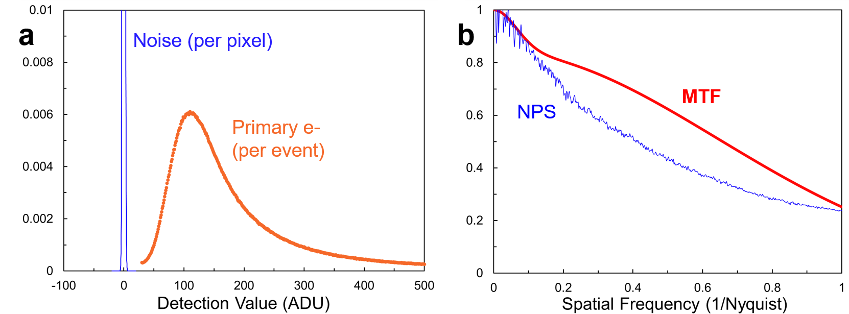
Figure 1: (a) Histograms of background noise per pixel per frame in the absence of incident electrons and the total signal deposited in the detector by incident 200 kV primary electrons in rolling shutter high-gain mode at ~1800 fps. (b) MTF and noise power spectrum (NPS) for 200 kV electrons.


Uncaptioned visual

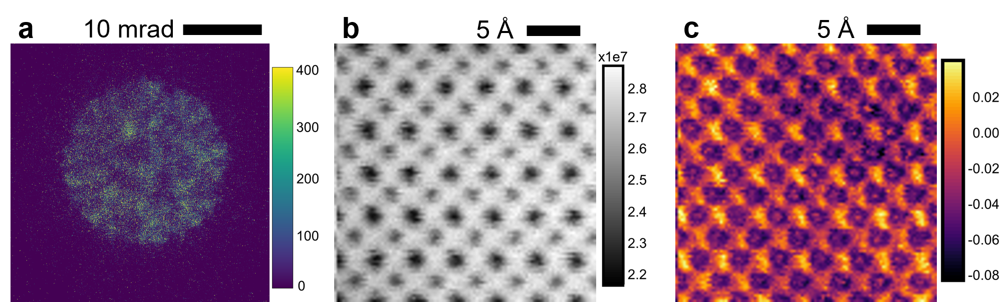
Figure 2: 4D STEM data acquired with Celeritas from a SrTiO3 sample at ~1,800 fps, full-frame. (a) A typical single frame CBED pattern. (b) A synthetic bright-field STEM image. (c) A 90-degree symmetry STEM image. The color scales in (a) and (b) are in detector counts. The color scale in (c) is the value of the symmetry coefficient.

Keywords

Direct Detection

4D STEM

Ultrafast

References

[1]      C. Ophus, Microsc. Microanal. 25, 563 (2019).

[2]      L. Zhou, et. al. Nat. Commun. 11, 2773 (2020) .

[3]      Y. Jiang, et. al., Nature 559, 343 (2018).

[4]      M. Krajnak, J. Etheridge, Proc. Natl. Acad. Sci. 117, 27805 (2020).

[5]      B.D.A. Levin, et. al. , Microsc. Anal. 34(1), 20 (2020).

[6]      A.B. Yankovich, et. al.  Nat. Commun. 5, 4155 (2014).

[7]      X. Sang, J. M. Lebeau, Ultramicroscopy 138, 28 (2014).

[8]      L. He, et. al., Microsc. Microanal. 21, 1026 (2015).


10:42 - 10:54

257 On the Dependence of the Sensitivity of EELS vs XEDS in the AEM with Thickness and Beam Energy

Andrew B. Yankovich1, Lunjie Zeng1, Eva Olsson1, Nestor J. Zaluzec2,1
1Dept. of Physics, Chalmers University of Technology, Gothenburg, Sweden. 2Photon Sciences Directorate, Argonne National Laboratory, Argonne, Illinois, USA

Abstract Text

The relative sensitivity of X-ray Energy Dispersive Spectroscopy (XEDS) and Electron Energy Loss Spectroscopy (EELS) has been studied for years by the Analytical Electron Microscopy community [1]. It is well accepted that the absolute signal generation of EELS compared to XEDS is fundamentally greater. However, the variation of the relative sensitivity of the techniques as defined by an unbiased measure has rarely been reported. In this work we have measured the variation in Signal & Background for both EELS and XEDS as a function of thickness and accelerating voltage and use it to show that a figure of merit can be used to compare the two spectroscopies.


The experimental XEDS and EELS data herein were obtained from the regions of an ion milled single crystal specimen of Nickel Oxide (NiO). The spectral data sets were measured simultaneously under identical non-channeling conditions of thickness, beam current, time, and accelerating voltage using a monochromated, image and probe corrected JEOL MonoNEOARM 200F, equipped with dual silicon drift detectors for XEDS, and a Gatan GIF Continuum HR system for EELS at 60 and 200 kV. In Figure 1, we plot representative spectra from the NiO specimen at two relative thicknesses (t/λ). The Oxygen K and the Nickel L data are shown in the respective EELS (Figure 1A) and XEDS (Figure 1B) data. The same spectral data is replotted in Figure 1C and 1D, however it is normalized to the pre-Oxygen background, which highlights the important difference namely the change in the Signal/Background (IS/IB) ratio, which affects the sensitivity and the minimum mass fraction (MMF). [2]


Uncaptioned visual

Figure 1) Comparison of EELS (A & C) and XEDS (B & D) showing the O K and Ni L signals for two values of t/λ A & B are raw data, while C & D are normalized to the O K background values


In Figure 2 we illustrate this more succinctly by plotting the experimentally measured IS/IB ratio as a function of both relative thickness and accelerating voltage. In this figure we can see that the EELS signal/background varies by as much as 200% compared to < 15% for XEDS. The thickness normalized MMF, is an inverse function of 


Uncaptioned visual


 thus although the raw signal for EELS is significantly better than that of XEDS, the severe background created by multiple inelastic scattering dramatically reduces the advantage of EELS over XEDS for thicker specimens. By contrast, the IS/IB ratio in XEDS is relatively constant owing to the fact that both the characteristic and background signals vary nearly linearly with thickness over the regime tested here (t/λ < 3).


.A close up of a map

Description automatically generated

Figure 2) Experimental variation in the Signal/Background for EELS (A) and XEDS (B) measurements as a function of relative thickness at 60 and 200 kV. Solid lines are guides to the eye for the 200 kV data.

 With the advent of new high solid angle XEDS systems, the increased signal for XEDS can bring an advantage to this spectroscopy in thicker specimens when only elemental spectroscopy is being conducted. This is best appreciated using a thickness normalized value for the MMF, which can be shown to be:


Uncaptioned visual

This work was supported in part by the Material Science Area of Advance and Excellence Initiative Nano at Chalmers University of Technology, the Swedish Research Council (VR) under Grant No. 2016‐04618, the European Union's Horizon 2020 research and innovation program under grant agreement No.823717‐ESTEEM3 and by the U.S. Department of Energy, Office of Science, Office of Basic Energy Sciences under Contract No. DE-AC02-06CH11357


Keywords

XEDS, EELS,  sensitivity, AEM, TEM, STEM

References

[1] Fraser H, Klenov D., Wang Y., Cheng H.  Zaluzec N.J,  Microsc. Microanal. 17 (Suppl. 2), 2011 590-591 

[2] Zaluzec N.J., Ultramicroscopy 203 (2019) 163–169 


10:54 - 11:06

32 Increasing the Usable Frame-rate of your Existing STEM

Dr Jonathan Peters1,2, Tiarnan Mullarkey1,2, Clive Downing2, Dr Lewys Jones1,2
1School of Physics, Trinity College Dublin, Dublin, Ireland. 2Advanced Microscopy Laboratory, CRANN, Dublin, Ireland

Abstract Text

Scanning transmission electron microscopy has increasingly become the preferred imaging mode in TEM due to its intuitive interpretation and ability to collect multiple signals simultaneously. However, the serial nature of STEM gives rise to several limitations that must be considered in any experiment. STEM is vulnerable to sample drift effects, presenting as non-rigid distortions in an image [1], and the high local beam current density and the resulting electron dose rate is capable of damaging many technologically interesting specimens. Recent developments in in-situ microscopy have led to the desire to capture dynamic events at high frame rates. Current scanning speeds attainable in typical STEMs are on the order of seconds for a 512x512 image, leading to a high probability of distorted images of beam damaged samples with low temporal resolution.

All of these problems can be mitigated by increasing the scan speed when imaging. The acquisition time of a single STEM image results from several variables: the pixel count, the pixel dwell time and the line flyback time. Decreasing the pixel count is an easy way to increase STEM frame rates, but often comes with an unacceptable penalty to resolution and/or field of view. Minimum usable pixel dwell times are typically limited by detector afterglow and the control electronics, with values on the order of 1 μs typically achievable [2]. Flyback waiting time is to account for the hysteresis in the scan coils arising from induction effects in the scan coils [3]. The Flyback time is typically on the order of 500 μs, and can account for a significant proportion of the image acquisition time. While is it possible to use improved hardware to reduce flyback hysteresis or dwell times, this presents a price hurdle and potentially disrupts integration into existing hardware and/or software [4].

Here we present a methodology to increase the achievable framerates of a Gatan Digiscan II controlling a Nion UltraSTEM. Through a careful, one-time calibration of the hysteresis behaviour of the scan system, we are able to correct for this in real time at the microscope. We show that our high framerate acquisition does not present any loss of precision through distortion analyses. Finally, we discuss the remaining limitations on STEM frame rates and strategies for future improvement.

Keywords

STEM, Frame rate, Real time, Dose rate, Precision

References

[1] L. Jones, H. Yang, T. J. Pennycook, M. S. J. Marshall, S. Van Aert, N. D. Browning, M. R. Castell, and P. D. Nellist, Adv. Struct. Chem. Imaging 1, 8 (2015).
[2] T. Mullarkey, C. Downing, and L. Jones, Microsc. Microanal. 27, 99 (2020).
[3] J. P. Buban, Q. Ramasse, B. Gipson, N. D. Browning, and H. Stahlberg, J. Electron Microsc. (Tokyo). 59, 103 (2010).
[4] R. Ishikawa, Y. Jimbo, M. Terao, M. Nishikawa, Y. Ueno, S. Morishita, M. Mukai, N. Shibata, and Y. Ikuhara, Microscopy 69, 240 (2020).


11:11 - 11:14

143 Atomic scale 3D reconstruction of nanostructures using inline 3D holography

Mr Pritam Banerjee1, Mr Chiranjit Roy1, Mr Subhra Kanti De1, Mr Antonio J. Santos2, Dr Juan Jesús Jiménez2, Dr Francisco M. Morales2, Dr Somnath Bhattacharyya1
1Department of Metallurgical and Materials Engineering, Indian Institute of Technology Madras, Chennai, India. 2Department of Materials Science and Metallurgic Engineering, and Inorganic Chemistry, Faculty of Sciences, University of Cádiz, Cádiz, Spain

Abstract Text

Nanostructures have a wide range of applications due to their unique geometry and arrangement of atoms. For a precise structure-property correlation, information regarding atomically resolved 3D structures of the nanostructure is of utmost beneficial. Though modern aberration-corrected transmission electron microscopes can resolve atoms with the sub-angstrom resolution, an atomic-scale 3D reconstruction of the nanostructure is a challenge using tilt series tomography due to high radiation damage. Instead, inline 3D holography based tomographic reconstructions from single projection registered at low electron doses is more suitable for defining atoms dispositions at nanostructures. Nanostructures such as nanoparticles are generally supported on amorphous carbon film for TEM experiments. However, neglecting the influence of carbon film on the tomographic reconstruction of the nanoparticle may lead to ambiguity. In order to address this issue, the effect of amorphous carbon support was quantitatively studied using simulations and experiments and it was revealed that increasing thickness and/or density of carbon support increases distortion in tomograms. The inline 3D holography technique was also implemented on InN QDs (<10 nm) grown on a Si substrate. The residual amorphous glue which acts similarly as amorphous carbon distorts the exit surface geometry, hence an error correction method was proposed. The pre-pyramid shape of QD sized below 10 nm was experimentally determined that supports theoretical predictions.

Keywords

InN quantum dot, nanoparticle, Inline-3D-holography, electron tomography, electron channelling theory

References

  1. Pritam Banerjee, Chiranjit Roy, Subhra Kanti De, Antonio J. Santos, Francisco M. Morales, Somnath Bhattacharyya, “Atomically resolved tomographic reconstruction of nanoparticles from single projection: Influence of amorphous carbon support”, Ultramicroscopy, Volume 221, 2021, 113177. https://doi.org/10.1016/j.ultramic.2020.113177

11:17 - 11:20

242 An efficient solution for correlative microscopy and co-localized observations based on multiscale multimodal machine-readable nanoGPS tags

Dr Sebastien Legendre1, Dr Olivier Acher2, Dr Raghda Makarem1, Dr Thanh-Liêm Nguyên2
1HORIBA FRANCE SAS, Loos, France. 2HORIBA FRANCE SAS, Palaiseau, France

Abstract Text

Investigating the same regions of interest of a sample with different instruments has for long been recognized as a very useful approach in various scientific fields. This presentation presents an original solution to spot the same points of interests on different microscopes with a high degree of accuracy and simplicity. It is based on small patterned tags fixed on the samples or their substrates. The patterns include an imaged-based position sensing technology, for which an image of a small part of the tag can be automatically interpreted into absolute coordinates and angular orientation. Taking a single snapshot on the tag with an imaging instrument provides the correspondence between sample and moving stage coordinates. Co-localized observations performed with scanning electron microscopes, optical microscopes and Raman microscopes are presented. Accuracy is in the few μm up to 20 μm range, which is generally sufficient to remove any ambiguity between the observed objects. The different contributions to colocalization errors are investigated experimentally. It is shown that the errors related to the tags are negligeable and that the main source of error is related to the accuracy of the moving stage integrated in the microscopes. An estimator of the relocalization error can be obtained in a straightforward way. This solution is believed to save time to researchers and facilitate cooperation between laboratories.

Keywords

correlative microscopy, colocalization, relocalization, technique hyphenation, Raman-SEM

References

Olivier Acher et al 2021 Meas. Sci. Technol. 32 045402
https://doi.org/10.1088/1361-6501/abce39


11:25 - 11:37

206 Three-dimensional imaging of a single impurity atom inside a thick crystal using multislice electron ptychography

Prof David Muller
Cornell University, Ithaca, USA

Abstract Text

The ultimate limit to spatial resolution in an electron microscope is set by the thermal vibrations of the atoms themselves, which are on the order of 10-20 pm [1]. Using multislice electron ptychography, we are surprisingly close to this limit. Although conventional annular dark-field imaging has reached spatial resolutions better than 50 pm [2,3], such performance can only be realized in thin samples, usually only a few nanometers thick and after the correction of high-order aberrations. In thicker samples, strong multiple scattering changes the probe shape and causes dechannelling effects between neighboring atomic columns which reduces the interpretable resolution [4]. Multiple scattering also leads to a complicated image contrast that is nonlinearly or even nonmonotonically dependent on the sample thickness, especially for phase-contrast imaging methods.

 Ptychography uses scanning diffraction and 4D-STEM datasets to iteratively reconstruct the electrostatic potential and has reached a resolution of 39 pm in thin 2D materials [5]. However, conventional ptychography (single-slice) assumes that the exit-surface wave function can be expressed as a multiplication of the incident probe and a single complex transmission function whose phase represents the sample projected potential. This approximation usually fails for samples thicker than a few nanometers in the presence of strong multiple scattering. For thick samples, attempts at phase retrieval from both multi-slice electron ptychography [6-8] and Bloch wave based scattering matrix [9] approaches have been reported. However, to date, none of the experimental demonstrations have been widely adopted due to limited resolution or image quality.

Here, we demonstrate a robust experimental realization of inversion of the multiple scattering using a regularized implementation of multislice electron ptychography [10]. This approach provides ultra-high-resolution reconstructions for samples hundreds of Angstroms thick (Figure 1(a)). More importantly, the contrast maintains a linear dependence on thickness over a wide thickness range. The linear phase-contrast can also greatly widen the applicable sample thickness and makes it possible to obtain three-dimensional structural information including the locations of single dopant and interstitial atoms (Figure 2).

The potential reconstructed from multislice ptychography from an experimental dataset acquired from a 21-nm-thick PrScO3 sample (Figure 1a), similar to that from a simulated dataset shows only a slight additional blurring compared to the potential at 300 K (Figure 1c). The diffractogram of the phase image shows an isotropic information transfer up to 4.39 Å-1, corresponding to 23 pm in real space. Quantitative analysis of the atomic column width reveals that the blurring from the instrument is smaller than 20 pm, which is smaller than the intrinsic broadening from thermal fluctuations. The method also allows for direct measurements of Debye-Waller factors of atoms near defects or interfaces [11].


A screenshot of a computer

Description automatically generated with medium confidence

Figure 1. Lattice-vibration-limited resolution from multislice ptychography. (a). Multislice ptychographically-reconstructed phase image from an experimental dataset acquired from a 21 nm thick PrScOsample. (b) static potential neglecting zero-point fluctuations, (c) Projected Potential calculated including thermal vibrations at 300 K. (d) Diffractogram of the phase image from experiment and (e) a line profile cut through d on a log scale.

Uncaptioned visual

Figure 2. (a) Multislice ptychographic reconstruction of a Gd3Ga5O12 film near an interface with Tm3Fe5O12. Phase image at depths z=4 nm (b) and z=6 nm (c) within the blue box from (a).  The red and blue arrows mark the location of an interstitial Tm atom 2nm apart in depth. (d) Depth variation of phase intensity across one dopant along a cut in the vertical direction. The data was acquired using a probe-forming semi-angle of 21.4 mrad at 300 kV.

Keywords

 Detector Technologies and New Instrumentation,
 Phase Sensitive Techniques,
4D-STEM,

Ptychography

References

[1] MA O’Keefe, Ultramicroscopy 108 (2008), p. 196-209.

[2] R Erni, et al., Physical Review Letters 102 (2009), p. 096101.

[3] H Sawada, et al., Journal of Electron Microscopy 58 (2009), p. 357-361. 

[4] R Hovden, et al., Physical Review B, 86 (2012), p. 195415.

[5] Y Jiang, et al., Nature 559 (2018), p. 343.

[6] S Gao, et al., Nature Communications 8 (2017), p. 163.

[7] Y Jiang, et al., Microscopy and Microanalysis 24 (2018), p. 192-193.

[8] M Schloz, et al., Optics Express 28 (2020), p. 28306-28323.

[9] HG Brown, et al., Physical Review Letters 121 (2018), p. 266102. 

[10] Z Chen, et al., arXiv: 2101.00465 (2021).

[11] Research supported by US NSF (grants DMR-1539918 and DMR-1719875). Research conducted by  Zhen Chen, Yi Jiang, Yu-Tsun Shao, Megan E. Holtz, Michal Odstrčil, Manuel Guizar-Sicairos, Isabelle Hanke, Steffen Ganschow, Darrell G. Schlom, David A. Muller


11:37 - 11:49

46 Time correlation spectroscopy using event-driven data acquisition

Daen Jannis1,2, Prof. Dr. Knut Müller-Caspary3,4, Dr. Armand Béché1,2, Prof. Dr. Johan Verbeeck1,5
1EMAT, Antwerp, Belgium. 2NANOlab Center of Excellence, Antwerp, Belgium. 3Ernst Ruska-Centre, Jülich, Germany. 4RWTH Aachen University, Aachen, Germany. 5NANOlab Centre of Excellence, Antwerp, Belgium

Abstract Text

The abstract content is not included at the request of the author.


Keywords

Electron-energy loss spectroscopy, Energy-dispersive x-ray spectroscopy, Single event detection, Time correlation measurements

References

 [1] P. Kruit, H. Shuman, and A. P. Somlyo. Detection of X-rays and electron energy loss events in time coincidence. Ultramicroscopy, 13(3):205-213,1984.

[2] X. Llopart et al, Timepix, a 65k programmable pixel readout chip for arrival time, energy and/or photon counting measurements, Nucl. Instr. And Meth. A 581 (2007) 485-494

[3]  D. Jannis, K. Müller-Caspary, A. Béché, A. Oelsner and, J. Verbeeck, Spectroscopic coincidence experiments in transmission electron microscope, Appl. Phys. Lett. 114, 143101 (2019)

[4] The scan engine was designed by M. Tencé and M. Kociak from Université ParisSud, France. The device is currently being commercialised by Attolight. More in-formation can be obtained onhttps://attolight.com

[5] D.J., A.B. and J.V. acknowledge funding from the Flemish Research Fund FWO under project no. G093417N and G042920N, J.V. acknowledges funding from ESTEEM3, K.M.-C. acknowledges funding from Helmholtz grant VH-NG 1317 and FWO G042920N


11:49 - 11:52

91 Ultrafast nanoimaging of the order parameter in a structural phase transition

Till Domröse1, Thomas Danz1, Prof. Dr. Claus Ropers1,2
14th Physical Institute – Solids and Nanostructures, University of Göttingen, Göttingen, Germany. 2Max Planck Institute for Biophysical Chemistry, Göttingen, Germany

Abstract Text

Optical control strategies and modification of physical material properties induced by optical stimuli have a profound impact on current and future technological applications. Microscopically, the functionality of devices usually arises from the interplay of various degrees of freedom on nanometre length and femto- to picosecond time scales. However, drastic changes of material properties are often encoded in low-intensity signals, calling for new experimental means to explicitly access order parameters in out-of-equilibrium scenarios.

Ultrafast transmission electron microscopy (UTEM) promises insights into ultrafast processes in heterogeneous structures by means of imaging, diffraction, and spectroscopy [1]. In the Göttingen UTEM, we use ultrashort electron pulses generated by linear photoemission from a nanometric tip emitter to investigate out-of-equilibrium dynamics in laser pump/electron probe experiments [2]. The exceptional beam properties allow for a versatile use of the Göttingen UTEM, as demonstrated in recent years [3-10].

A particularly intriguing application of UTEM is the investigation of structural phase transitions such as in the prototypical charge-density wave (CDW) material 1T-TaS2, which have been studied in various ultrafast diffraction experiments in the past [11-14]. The structural state of this material is encoded into a subtle additional periodic modulation of the crystal structure accompanying CDW formation, constituting various first-order phase transitions ranging from an insulating state at low temperatures to a metallic high-temperature phase [15].

In this work, we demonstrate a new experimental approach to image the structural phase transition from the semi-metallic, nearly commensurate (NC) CDW modification of 1T-TaS2 at room-temperature to the metallic, incommensurate (IC) CDW at higher temperatures in real space with 5-nm spatial and femtosecond temporal resolution (see Fig. 1A for a schematic of the experimental setup) [16]. By introducing a specifically tailored dark-field aperture array (Fig. 1B), we gain sensitivity to the local CDW periodicity of the NC CDW phase in the presence of spatially inhomogeneous optical excitation in the 1T-TaS2 thin film [17]. Initially, we witness a global quench of the NC CDW amplitude governed by the local fluence of the optical pump beam, followed by a condensation of IC CDW domains (see Fig. 2A for the resulting micrographs). Specifically, our approach allows us to analyse dynamics in the individual phases via image segmentation (Fig. 2B and C), and, furthermore, provides sensitivity to processes at domain walls, where we observe a sharpening within a few picoseconds (Fig. 2D). Subsequently, the domain pattern evolves on the time scale of thermal diffusion, including an intermediate domain growth prior to the relaxation back to thermal equilibrium after a few nanoseconds.

In contrast, inducing the phase transition by continuous-wave laser excitation allows for a precise characterization of the thermal properties of our sample design. Based on this, we reproduce prominent features in the ultrafast dynamics in time-dependent Ginzburg-Landau simulations, elucidating relaxation pathways and domain wall dynamics

In conclusion, we demonstrate first ultrafast real-space imaging of a structural phase transition on its intrinsic time and length scales via a specifically tailored dark-field approach. Corroborated by a static specimen characterization and time-dependent Ginzburg-Landau simulations, we gain insights into order parameter dynamics at domain walls and thermal transport processes. As our experimental approach is easily transferred to other degrees of freedom in complex materials, we hope to inspire novel types of contrast-enhancement via beam-shaping in ultrafast methodologies.


Uncaptioned visual

Figure 1. Dark-field imaging in the ultrafast transmission electron microscope. (A) Experimental setup. Electron (green) and optical pulses (red) are incident close to perpendicular on the specimen. (B) Scanning electron micrograph of the tailored dark-field (DF) aperture array placed in the back-focal plane (BFP) in (A). (C) Electron diffractograms of the 1T-TaS2 thin film at room temperature with the DF aperture array shown in (B) retracted from (top) and inserted into the electron beam path (bottom). Only NC CDW superstructure reflections are transmitted through the aperture array [16].

Ein Bild, das Text enthält.

Automatisch generierte Beschreibung

Figure 2. Ultrafast dark-field domain imaging of charge-density wave dynamics. (A) Ultrafast DF micrographs of transient domain configurations in the 1T-TaS2 film obtained in the laser pump/electron probe scheme (2.6 mJ/cm2 pump fluence, linear pump polarization indicated by white arrow). Pump/probe delay steps were chosen to capture all major stages of the dynamics (see black circles above (C)). (B) Top: Image segmentation at 130 ps delay time. Bottom: The segmentation threshold is determined from the intensity histogram of the full image series within the circular aperture. (C) Top: Area fractions of NC and IC regions after completed phase separation, as determined from the segmented images. Bottom: Average intensity of the image series within the entire aperture (black curve), and average intensity in weakly and strongly pumped regions (green/orange curve; evaluated regions are indicated in (A) using corresponding colors). (D) Exemplary profiles of NC/IC phase boundaries taken on the white line indicated in (A). (E) Spatial profile of the excitation density giving rise to the initial suppression pattern [16].


Keywords

UTEM, Ultrafast, Transmission Electron Microscopy, Charge-density wave, Correlated materials, phase transition, 1T-TaS2, van-der-Waals material, Transition-metal dichalcogenides

References

  1. A. H. Zewail, Science 328, 187-193 (2010).
  2. A. Feist et al., Ultramicroscopy 176, 63-73 (2017)
  3. A. Feist et al., Nature 521, pp. 200-203 (2015).
  4. K. E. Priebe et al., Nat. Photonics 11, 793-797 (2017).
  5. A. Feist et al., Struct. Dyn. 5, 014302 (2018).
  6. N. Rubiano da Silva et al., Phys. Rev. X 8, 031052 (2018).
  7. N. Bach, T. Domröse, et al., Struct. Dyn. 6, 014301 (2019).
  8. M. Möller, et al., Commun. Phys. 3, 36 (2020).
  9. O. Kfir et al., Nature 582, 46-49 (2020).
  10. A. Feist et al., Phys. Rev. Research 2, 043227 (2020).
  11. M. Eichberger et al., Nature 468, 799-802 (2010).
  12. K. Haupt et al., Phys. Rev. Lett. 116, 016402 (2016).
  13. S. Vogelgesang et al., Nat. Phys. 14, 184-190 (2018).
  14. A. Zong et al., Sci. Adv. 4, eaau5501 (2018).
  15. K. Rossnagel, J. Phys. Condens. Matter 23, 213001 (2011).
  16. Th. Danz, T. Domröse, C. Ropers, Science 371, 371-374 (2021).
  17. Th. Danz et al., J. Phys. Condens. Matter 28, 356002 (2016).

11:52 - 11:55

5 Strain mapping using scanning precession electron diffraction - a round robin test of different methods for calculation from the raw datasets

Dr Ian MacLaren1, Ms Emma Devine1, Mr Hristo Gergov1, Dr Gary Paterson1, Dr Benjamin Savitzky2, Dr Colin Ophus2, Mr Renliang Yuan3, Prof Jian-Min Zuo3, Mr Harikrishnan K.P.4, Prof David Muller4, Ms Kirsten Forster1, Ms Gaja Kobe1, Ms Elizabeth Koppany1, Ms Kirsten McClymont1, Mr Anjelo Narendran1, Mr David Riley1
1University of Glasgow, Glasgow, United Kingdom. 2Lawrence Berkeley National Laboratory, Berkeley, USA. 3University of Illinois at Urbana-Champaign, Urbana, USA. 4Cornell University, Ithaca, USA

Abstract Text

Determining the strain in crystalline structures as a function of a position has been possible for some while with scanned nanobeam diffraction and scanning precession electron diffraction.  There are a number of ways to convert the diffraction patterns to strain maps, but there has been little by way of any attempt to evaluate or compare the relative merits of these different approaches.  This work examines two scanned precession diffraction datasets using five different analysis codes, which encompass some different approaches to the determination of spot positions and strain.  Direct comparisons will be made between all of these, and the reasons for the discrepancies that are found are examined, especially by analysing the diffraction pattern fits in pixels of the dataset where the largest differences are found between the different codes.  This will lead to clear recommendations as to the most appropriate techniques for strain mapping in different structures.

Keywords

4D-STEM

Precession Electron Diffraction

Direct Electron Detectors

Strain Mapping