To save this page as a PDF, click this button and choose the PDF destination.

Stream 1: EMAG - 4D-STEM

14:45 - 16:45 Thursday, 8th July, 2021

Sessions EMAG Conference Session

Session Organiser Donald Maclaren, Ana Sanchez


14:45 - 15:15

274 Uses of multimodal ptychography

Professor John Rodenburg, Mr Yangyang Mu
University of Sheffield, Sheffield, United Kingdom

Abstract Text

Ptychography overcomes three long-standing limitations that arise in all forms of transmission microscopy [1]. First, its resolution is not limited by the numerical aperture of the lens - in fact, it can work without any lenses at all. Second, it provides a very clean phase image (as well as a modulus image), without any ringing or Fresnel effects, while at the same time preserving low frequency structure in the image. Third, the phase image is strong and has high contrast, meaning that counts (radiation dose, and hence specimen damage) can be much smaller than for conventional imaging modes. 

The ptychographic principle has slowly gained traction, mostly because of the increase in the size and power of computers, and the vastly improved quality of detectors. The data used in ptychography involves processing hundreds or even thousands of diffraction patterns: information that is nowadays sometimes called ‘4D STEM data’. Inversion strategies to obtain continuous, infinite images began the early 1990s, but the technique was only adopted widely after about 2007.

This talk will briefly present an elementary introduction to ptychography for those who may not be familiar with it, or its potential powers and applications. It will review progress over all wavelengths.

Recent results will be presented, showing how it is possible to increase the speed of data acquisition in ptychography by appropriate engineering of the coherent modes in the illumination function (‘multi-modal’ ptychography), and by the subsequent use of modal decomposition [2]. This is demonstrated experimentally using synchrotron radiation, although it has potential applications over all wavelengths.


Keywords

ptychography, diffractive imaging, coherence, modal decomposition, X-ray microscopy, dose


15:15 - 15:27

11 In-situ biasing and temperature influence on the electric fields across GaAs based p-n junction via 4D STEM

Dr. Anuj Pokle, Mr. Damien Heimes, Dr. Andreas Beyer, Prof. Kerstin Volz
Philipps University Marburg, Marburg, Germany

Abstract Text

The ability to determine electric fields at the nanoscale quantitatively is critical for understanding semiconductor device properties. By employing transmission electron microscopy techniques like electron holography and differential phase-contrast imaging (DPC), fundamental aspects of the electron interaction with the electric potential field have been investigated 1,2. By performing in situ biasing, the effect of external voltages on GaAs and Si p-n junctions have also been investigated with electron holography 3,4. However, this approach requires a specialized setup where the primary beam is split into two, wherein the reference wave later interacts with the second wave passing via the specimen. 

Nevertheless, in recent times accessibility to direct electron detectors has enabled us to acquire four-dimensional datasets (diffraction patterns at each scan point), paving the way for new advanced developments. Here we combine in-situ biasing with a four-dimensional scanning transmission electron microscopy (4DSTEM) technique to study the influence on the depletion region in the GaAs-based p-n junction. In addition, the temperature influence on the electric fields is also investigated at liquid nitrogen temperature (~ -183 °C) to above room temperature (~50 °C). The biasing and temperature-dependent studies are conducted by incorporating an in situ biasing and a cryo holder, respectively. 

In this study, the momentum transfer induced by internal electric fields is measured by the diffraction pattern's center-of-mass (COM) shift 5. Identical imaging conditions are employed, which are used for obtaining high-resolution STEM images. Moreover, our sample preparation approach is based on the focused ion beam (FIB) method, which is nontrivial from the perspective of placing the lamella on the biasing MEMS chip. This enables us to determine the electrical properties for a known sample thickness observed from both biased and unbiased junctions followed by temperature application. Here we will show the biasing and temperature influence's critical characteristic on the depletion region width. 


Keywords

In-situ biasing, cryo, p-n junction, electric field measurements, FIB, 4D STEM and COM

References

1. Shibata, N. et al. Imaging of built-in electric field at a p-n junction by scanning transmission electron microscopy. Sci Rep 5, (2015).

2. McCartney, M. R., Dunin-Borkowski, R. E. & Smith, D. J. Quantitative measurement of nanoscale electrostatic potentials and charges using off-axis electron holography: Developments and opportunities. Ultramicroscopy 203, 105–118 (2019).

3. Twitchett, A. C., Dunin-Borkowski, R. E. & Midgley, P. A. Quantitative Electron Holography of Biased Semiconductor Devices. PHYSICAL REVIEW LETTERS 88, 4 (2002).

4. Anada, S. et al. Precise measurement of electric potential, field, and charge density profiles across a biased GaAs p-n tunnel junction by in situ phase-shifting electron holography. Journal of Applied Physics 122, 225702 (2017).

5. Beyer, A. et al. Quantitative Characterization of Nanometer-Scale Electric Fields via Momentum-Resolved STEM. Nano Lett. (2021) doi:10.1021/acs.nanolett.0c04544.


15:27 - 15:39

240 Ptychography on dynamically scattering samples

Dr Laura Clark1, Dr Gerardo Martinez2, Dr Colum O'Leary3, Dr Tim Petersen4, Dr Scott Findlay4, Prof Peter Nellist5
1University of Leeds, Leeds, United Kingdom. 2IMEC, Leuven, Belgium. 3University of California, Los Angeles, USA. 4Monash University, Clayton, Australia. 5University of Oxford, Oxford, United Kingdom

Abstract Text

Phase imaging of specimens in the STEM is becoming increasingly popular with the growing access to pixelated electron detectors – with relevant imaging techniques spanning across differential phase contrast (DPC) based methods and ptychographic techniques. Direct (non-iterative) electron ptychography in particular is rapid [1], dose-efficient [2] and can be run live at the microscope [3]. However, much of the theory is built upon the (weak) phase object approximation, and the projection approximation [4]. These criteria are strictly fulfilled by a limited subset of the samples we may wish to study. This naturally raises the question – how reliable are these methods when applied to the much wider classes of thicker specimens?

In this work, we present results from an investigation into applications of STEM phase imaging on a thickness-series of simulated data. Contrast from Wigner distribution deconvolution (WDD) and single sideband (SSB) ptychography remains on-column for dynamically scattering samples, beyond thicknesses where other methods lose column-resolution. This is confirmed with reference to experimental data. Furthermore, the ability to post-correct aberrations in experimental data allows for clear atomic-resolution images even when the collection conditions are not ideal –such as when collecting data on beam-sensitive samples. Following from this, we indicate the optimum focal conditions for collecting 4D-STEM phase imaging experimental data.

Simulations through a thickness series of GaN allow a comparison of conventional BF and DF images with (integrated) DPC, SSB and WDD ptychography. Analysis of the 4D Fourier transformed data of these simulations reveal aberrations in the dataset, minimised at a mid-sample focal condition as indicated in the figures below.


Uncaptioned visual


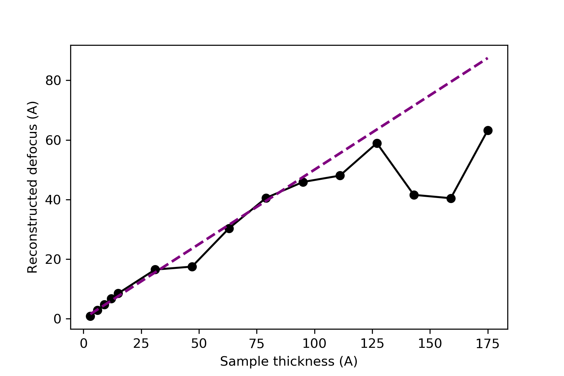
Figure 1: Reconstructed defocus analysis from a thickness series of GaN simulations (solid black line). Indication of defocus equal to thickness/2, purple dashed line. Data from the top surface focal condition, WDD analysis. 

Uncaptioned visual

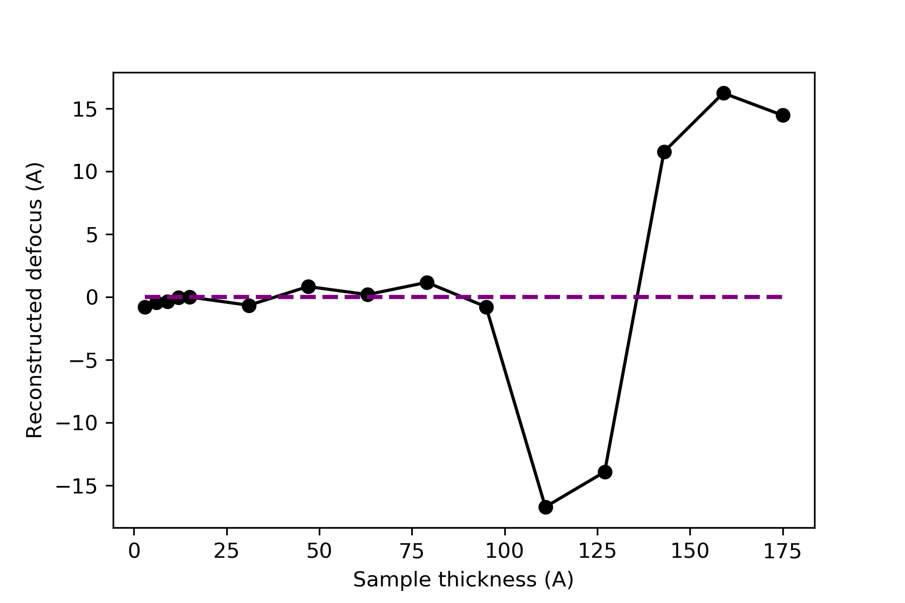
Figure 2: Reconstructed defocus analysis from a thickness series of GaN simulations (solid black line). Indication of defocus equal to zero, purple dashed line. Data from the midplane focal condition, WDD analysis.


Keywords

4D-STEM, DPC, ptychography, dynamic scattering, phase objects

References

[1] CM O’Leary et al. "Phase reconstruction using fast binary 4D STEM data." Applied Physics Letters 116.12 (2020): 124101.

[2] TJ Pennycook et al. "High dose efficiency atomic resolution imaging via electron ptychography." Ultramicroscopy 196 (2019): 131-135.

[3] K Muller-Caspary, “Momentum-resolved STEM: An interdisciplinary methodological platform for materials and soft matter characterization.” RMS Virtual Microscopy Characterisation of Organic-Inorganic Interfaces, 12th March 2021.

[4] M Vulović et al. "When to use the projection assumption and the weak-phase object approximation in phase contrast cryo-EM." Ultramicroscopy 136 (2014): 61-66.


15:39 - 15:51

89 Improved magnetic field mapping of Fe60Al40 embedded nanomagnets by precession-corrected STEM-DPC

Mr Gregory Nordahl1, Dr Damien McGrouther2, Dr Magnus Nord1
1Department of Physics, Norwegian University of Science and Technology, Trondheim, Norway. 2School of Physics and Astronomy, University of Glasgow, Glasgow, United Kingdom

Abstract Text

In scanning transmission electron microscopy (STEM), a useful technique for quantitative analysis of ferromagnetic domains is differential phase contrast (DPC). A necessity for this technique is a detector geometry that can record electron beam phase shifts in the diffraction plane, described by the Aharonov-Bohm effect [1]. Segmented detectors have previously been the go-to choice, however, the advent of fast pixelated direct detection technology has made 4D-STEM possible [2], with one of the outcomes being improved imaging of magnetic fields by the STEM-DPC technique [3]. With this detector technology, structural information can be extracted simultaneously in conjunction with magnetic information, given that the selected camera length is low enough [4].

Since magnetic information is typically extracted from the bright field disk containing the unscattered electrons, anything that can disrupt the uniformity of the central disk may lead to unreasonable estimation of the field strength or direction, or even present magnetic contrast where there should be none. Contrast mechanisms other than magnetic, such as diffraction contrast due to local crystal orientation or dynamical diffraction effects, are often unavoidable causes of beam inhomogeneity [3]. An example illustrating artefacts in STEM-DPC imaging resulting from Bragg diffraction can be seen in Figure 1. A good representation of an undisturbed bright field disk can be seen in (b), while (c) shows the effect of inhomogeneities due strong Bragg diffraction on the bright field disk, which result in artefacts as seen in (d).

In this presentation, we will present our work utilizing beam precession as means to alleviate diffraction contrast artefacts in STEM-DPC data. The quality of structural information contained in diffraction spots is also improved by precession, due to a larger degree of diffraction space sampling and reduction in dynamical diffraction effects [5]. Similar studies have been performed where precession-corrected STEM-DPC have been used to study electric fields [6]. Studying magnetic fields with STEM-DPC, however, requires the objective lens to be turned off as to not saturate the magnetic structure immersed in the lens field. The technique is applied on Fe60Al40 ferromagnetic nanostructures embedded in a non-ferromagnetic film. The film matrix, an ordered, paramagnetic B2 structure, is irradiated by Ne+ ions to create desired shapes of disordered, ferromagnetic A2 structure, with a slightly increased unit cell parameter [4]. Figure 1(a) shows a STEM-DPC image of a ring-shaped ferromagnetic structure, created by Ne+ ion irradiation of a Fe60Al40 film. The work was performed on a non-corrected JEM-2100F, equipped with a MerlinEM fast pixelated detector and a NanoMEGAS DigiSTAR instrument for precession control.

Uncaptioned visual

Figure 1. (a) STEM-DPC image of an embedded, ring-shaped ferromagnetic structure in Fe60Al40. Different colored regions correspond to ferromagnetic domains, with color wheel showing direction and magnitude of magnetization. Image of bright field disk from a region (b) without strong Bragg diffraction and (c) with strong Bragg diffraction. (d) STEM-DPC image of single-crystalline magnetic thin film. Bragg diffraction effects caused from structural variations are interpreted as magnetic beam shifts, leading to artefacts resembling magnetic fields.

Keywords

4D-STEM

STEM-DPC

Precession

References

[1] J. N. Chapman, I. R. McFadyen, S. McVitie, IEEE Trans. Magn. 26, 1506 (1990).

[2] C. Ophus, Microsc. Microanal. 25, 563 (2019).

[3] M. Krajnak, D. McGrouther, D. Maneuski, V. O’Shea, S. McVitie, Ultramicroscopy. 165, 42 (2016).

[4] M. Nord, A. Semisalova, A. Kákay, G. Hlawacek, I. MacLaren, V. Liersch, O. M. Volkov, D. Makarov, G. W. Paterson, K. Potzger, J. Lindner, J. Fassbender, D. McGrouther, R. Bali, Small. 15, 1904738 (2019).

[5] P. A. Midgley, A. S. Eggeman, IUCrJ. 2, 126 (2015).

[6] L. Bruas, V. Boureau, A. P. Conian, S. Martinie, J. L. Rouviere, D. Cooper, J. Appl. Phys. 127, 205703 (2020).


15:56 - 15:59

151 Optimal experiment design for characterising structures containing multiple types of elements using 4D scanning transmission electron microscopy

Duygu Gizem Sentürk1,2, Annick De Backer1,2, Sandra Van Aert1,2
1EMAT, University of Antwerp, Antwerp, Belgium. 2NANOlab Center of Excellence, University of Antwerp, Antwerp, Belgium

Abstract Text

Aberration corrected scanning transmission electron microscopy (STEM) has become a powerful technique for materials characterisation of complex nanostructures. In combination with quantitative methods, structural information such as number of atoms can be retrieved from experimental images. To obtain reliable atom-counting, one can predict the optimal experimental settings. For this purpose, the probability of error (Pe) concept was introduced [1,2] using statistical detection theory that enabled us to find the optimal detector collection regions to count the number of atoms from monotype nanosystems. To extend the problem for the investigation of complex hetero nanostructures, the use of pixelated detectors offers important advantages since it allows us to create conventional STEM images with any number of virtual detectors without the need for pre-configured fixed detector angles [3] or ultimately to use the full 4D STEM dataset. 

In the present work, we have extended the concept of the Pe to investigate the potential benefit of analysing multiple 2D STEM images when counting atoms of different chemical nature. In this methodology, the atom-counting problem is formulated as a statistical hypothesis test, where each hypothesis corresponds to a specific number of atoms in an atomic column. The Pe corresponds to the probability to choose the wrong hypothesis. To compute the Pe, realistic 4D STEM simulations were performed from which multiple 2D STEM images were generated with varying inner and outer detector angles. From these 2D images, so-called scattering cross-sections (SCS) can be computed corresponding to the total scattered intensity for each atomic column. This measure has been shown to perform as an optimal criterion for atom-counting [2]. Moreover, the presence of electron counting noise is taken into account when computing the Pe. 

To illustrate the concept, the Pe has been calculated to distinguish between pure Ag and Au columns up to 20 atoms thick for SCSs for an incident electron dose of 104 e-2. In Figure 1a, the red curve shows the evaluation of the Pe as a function of the outer angle of a single ADF detector with a fixed inner angle, while the blue curve shows the evaluation as a function of the inner angle with a fixed outer angle. From these results, it follows that the optimal Pe equals 16% when using a single ADF detector. The yellow curve represents the calculation of the Pe for the combination of scattering cross-sections extracted from two non-overlapping detectors. This clearly shows that the Pe can be reduced to only 2% when two sets of independent data are employed. In Figure 1b, the Pe is evaluated as a function of the electron dose under the optimal detector settings for a single ADF detector, for a combination of two optimal independent detectors, and for the full dark field region of the 4D STEM dataset. The dashed horizontal line shows that when aiming for a Pe as low as 2%, the electron dose can be further reduced to 103 e-when exploring the 4D STEM dataset.

Subsequently, the research problem was extended to a Au@Ag core-shell nanoparticle to retrieve information about different types of elements in a binary mixed atomic column structure with minimum Pe. In this research problem, the total thickness of the Au-Ag mixed atomic columns varies from 1 up to 20 atoms and the core is assumed to be located in the centre. The Pe has been calculated to distinguish both the total number of atoms in the atomic column and the number of Au atoms in the core. In Figure 2a, the Pe is evaluated as a function of the detector angles for an incident electron dose of 10e-2 resulting in a higher Pe as compared to the previous study for pure columns up to 20 atoms thick. However, in this case, the Pe can be reduced from 65% to 15% when a combination of two ADF detectors is employed rather than a single optimal ADF detector. In Figure 2b, the evaluation of the Pe as a function of the incident electron dose is shown. The dashed horizontal line shows that to reach a Pe of 2%, the electron dose can be reduced by a factor of 103 when using two optimal non-overlapping detectors. Consequently, the required electron dose to count the number of atoms for different types of elements in a binary mixed atomic structure can significantly be lowered with the use of two independent 2D STEM images reconstructed from a 4D STEM dataset.

In summary, we have shown that the concept of the Pe can be used to find optimal strategies to count atoms from 4D STEM datasets. In particular, the method is generalised to create a set of multiple 2D STEM images providing independent information concerning thickness, composition, and ordering of the atoms along the viewing direction [4].

Uncaptioned visual

Figure 1: Pe to distinguish between pure Ag and Au columns (a) as a function of the outer angle of a single ADF detector with fixed inner angle (red), the inner angle of a single ADF detector with fixed outer angle (blue), and the common angle x for two independent detectors (yellow) for an incident electron dose of 104 e-2 (b) Pe as a function of the incident electron dose calculated for a single ADF detector (blue), two independent ADF detectors (yellow), and for the full dark field region of the 4D STEM dataset (green).

Uncaptioned visual

Figure 2: Pe for Au@Ag core-shell nanoparticle to distinguish between the total number of atoms and type of atoms in a binary mixed atomic column varying from 1 up to 20 atoms (a) as a function of the outer angle of a single ADF detector with fixed inner angle (red), the inner angle of a single ADF detector with fixed outer angle (blue), and the common angle x for two independent detectors (yellow) for an incident electron dose of 104 e-2 (b) Pe as a function of the incident electron dose calculated for a single ADF detector (blue) and two independent ADF detectors (yellow).

References

[1] J. Gonnissen et al., Appl. Phys. Lett. 105 (2014) 063116

[2] A. De Backer et al., Ultramicroscopy 151 (2015) 46

[3] N. Shibata et al., J. Electron Microsc. 59 (2010) 473 

[4] This work was supported by the European Research Council (Grant 770887 PICOMETRICS to SVA and Grant 823717 ESTEEM3). The authors acknowledge financial support from the Research Foundation Flanders (FWO Belgium) through project fundings and a postdoctoral grant to ADB.


15:59 - 16:02

225 In-STEM Transmission Kikuchi Diffraction of nanoscale crystalline defects in zirconium alloys

Dr Jack Haley1, Dr Phani Karamched1, Dr Philipp Frankel2, Prof Chris Grovenor1
1University of Oxford, Oxford, United Kingdom. 2University of Manchester, Manchester, United Kingdom

Abstract Text

The degradation of zirconium-based fuel cladding in light water nuclear reactors is responsible for fuel rods being removed prematurely, before the entire fissionable uranium has been spent.  This means a large quantity of fuel goes unused in light water reactors, leading to increased waste and reduced economic efficiency. Hence, the development of new zirconium alloys, and an improvement to our understanding of the degradation mechanisms, would allow for a longer lifetime for fuel rods. We have been using transmission electron microscopy to learn more about the changes that occur to zirconium alloys during service, with particular focus on both changes to the local chemistry, and the evolution of irradiation-induced dislocations in the microstructure.


Transmission Kikuchi Diffraction is a technique more commonly associated with SEMs, but in this presentation, we will show how it can be used in-STEM to rapidly characterise complicated irradiation-damaged microstructures. The availability of fast-pixelated-cameras means maps of the precise plane orientation around individual crystalline defects can be made in minutes, and in a fashion comparable to taking Bright field or Annular Dark field images. This wealth of crystallographic information that in-STEM TKD brings has never before been so convenient to the microscopist. 


We have used this in-STEM TKD method to produce quantitative measurements of the lattice distortion cause by nanoscale dislocation loops with precision down to fractions of a degree. This allows us to directly compare the simulated displacement field with the measured misorientation, without any of the complexity of diffraction contrast. On a larger scale, we have used misorientation maps to calculate the Geometrically Necessary Dislocation (GND) density, calibrated against HR-EBSD, allowing a novel method for quantifying radiation damage from the measured lattice distortion, without needing to count a single dislocation. 

Uncaptioned visual


This research used UKAEA’s Materials Research Facility, which has been funded by and is part of the UK’s National Nuclear User Facility and Henry Royce Institute for Advanced Materials.

Keywords

TKD, 4D-STEM, radiation damage, zirconium, dislocation loops


16:02 - 16:05

338 Design of electron ptychography experiments through simulations

Dr. Mohsen Danaie1, Dr. Darren Batey2, Dr. Thomas Slater1, Dr. Christopher Allen1,3
1Diamond Light Source Ltd., electron Physical Science Imaging Centre (ePSIC), Didcot, United Kingdom. 2Diamond Light Source Ltd., Didcot, United Kingdom. 3University of Oxford, Oxford, United Kingdom

Abstract Text

With the wider accessibility of fast direct-electron detectors, collecting electron diffraction patterns in the scanning mode of the transmission electron microscope is becoming common place. These datasets – also known as 4D-STEM, with two dimensions on the scan array and two on the detector plane containing the diffraction corresponding to a given probe position – can be used to reconstruct both the complex object and the probe using ptychographic algorithms. Solving for the object via ptychography, in principle, can relax the requirements on the optical hardware to achieve atomic resolution imaging1 and has also been shown to be beneficial in reducing the total dose received by the sample2. Given the large number of parameters that the experimentalist operating a modern electron microscope can vary, carrying out an electron ptychography experiment, while ensuring that the collected data is conducive to a satisfactory reconstruction, can at times be a daunting task. Here we present a workflow to simulate a matrix of optical and sampling conditions to provide feedback on the optimal conditions to be used for the electron ptychography experiment. As there are various ptychographic reconstruction algorithms with different sampling criteria, our focus here is the extended ptychographical iterative engine (ePIE) implemented by one of the present authors in the ptyREX python library3


The workflow used in this study is presented in the schematic shown in Figure 1. The atomic model corresponding to the phase under investigation is imported to the Prismatic simulation package in python, and a multislice simulation is performed with the 4D-STEM output saved4. Python interface allows systematic variation in the input parameters of the optics such as probe convergence semi-angle, probe aberrations and also the probe step size in the simulated data. This data is then modified to incorporate noise and electron dose and fed into the ptyREX reconstruction algorithm. Following the ePIE reconstructions we then evaluate the outcomes based on a set of quantitative metrics. This allows us to identify the optimal experimental parameters for a given set of metrics used.


Uncaptioned visual

Figure 1. Workflow for evaluating a set of parameters in an electron ptychography experiment.


As a case study, we looked at a graphene atomic model with some defects included in the structure. With the probe defocus set to result in roughly the same probe diameter in each case, we varied the sampling in the real space and diffraction discs overlap in reciprocal space, by changing the probe step size and the probe convergence semi-angle, respectively. The reconstruction outcome was then evaluated with comparison to the projected potential of the initial model. True positive (TP) cases were atomic positions in the reconstruction matched with one in the model, false negative (FN) cases defined as missing atoms in the reconstruction and false positives (FP) as atoms in the reconstruction where no atom is present in the model. These cases are presented with different colours in Figure 2 matrix. We used three quantitative metrics: (1) root-mean-squared error of the distances between the identified versus the known atomic positions, (2) Precision: TP / (FP + TP), and (3) Recall: TP / (FN + TP). Using these, we identify the optimal experimental parameter in this case as 50 mrad probe convergence angle with 80% real space probe overlap. This is close to what we have found experimentally at 80 kV.

Uncaptioned visual

Figure 2. The outcome of ePIE reconstruction for the simulated matrix of ptychographic data. The ground truth used for evaluation along with a legend of the matrix is shown on the right-hand side.


We are now exploring the robustness of ePIE reconstructions to the potential experimental errors in various input parameters. This would help identify the key critical parameters that require closer scrutiny for successful experiment. Our aim is to have this workflow implemented such that it is user-friendly as much as possible to provide Users at ePSIC a working framework to better design their electron ptychography experiments. 


References

1. J. Rodenburg and A. Maiden in P.W. Hawkes, J.C.H. Spence (Eds.), Springer Handbook of Microscopy, 2019.

2. J. Song, C. S. Allen, S. Gao, et al. Sci Rep 9, 3919 (2019). 

3. D. J. Batey, Ptychographic Imaging of Mixed States, Thesis, University of Sheffield (2014).

4. C. Ophus, Advanced Structural and Chemical Imaging 3(1), 13 (2017).


Keywords

ptychography, simulation


16:10 - 16:40

119 Quantification of light elements in ABF and 4D STEM electron ptychography

Dr Emanuela Liberti1,2,3, Dr Colum M. O'Leary2,4, Mr Kevin P. Treder2, Dr Judy S. Kim1,2,3, Prof Peter D. Nellist2, Prof Angus I. Kirkland1,2,3
1The Rosalind Franklin Institute, Harwell Campus, Didcot, United Kingdom. 2University of Oxford, Department of Materials, Oxford, United Kingdom. 3electron Physical Science Imaging Centre (ePSIC), Diamond Light Source, Didcot, United Kingdom. 4University of California, Los Angeles, USA

Abstract Text

Annular-dark field imaging is one of the most readily interpretable techniques in scanning transmission electron microscopy (STEM). The ADF detector integrates the intensity of incoherent, high-angle scattered electrons providing images with strong atomic number sensitivity that can be directly interpreted in terms of the sample’s atomic structure. The ADF contrast increases monotonically with the number of atoms in projection. This allows direct atomic counting to solve three-dimensional (3D) structures or determine composition at a given thickness [1 – 3]. However, ADF STEM is not efficient for light elements detection because they scatter less strongly at high scattering angles. More suitable methods to image both light and heavy atoms are based on bright-field or phase-contrast techniques that collect low-angle scattered electrons. However, because these electrons scatter coherently, image quantification, in this case, is non-trivial.

This talk will discuss quantification methods for two main (quasi-)coherent STEM imaging modes: annular-bright field (ABF) imaging and 4D STEM electron ptychography.

In the case of ABF, image quantification is applied to the characterisation of the oxygen framework in lithium-rich Li1.2Ni0.2Mn0.6O2 (LNMO) layered cathodes [4]. In this material, short-range oxygen sublattice distortions are evidence for oxygen participation in charge compensation mechanisms. These movements are of the order of picometres and, to be measured, require well-designed quantification methods. However, achieving picometre accuracy and precision is challenging in these materials because of the limited signal-to-noise ratio of the images imposed by the electron dose [5]. The first part of this talk discusses how to achieve high-quality ABF quantification using a combination of experimental design and computational data processing including simultaneous ADF atom counting and multi-slice image simulations. 

The second part of the talk shows how these methods can be extended to the quantification of 4D STEM electron ptychography data using fast electron detectors [6]. A four-dimensional dataset consist of a two-dimensional (2D) convergent beam electron diffraction pattern (CBED) recorded at every pixel of a 2D scan array. The exit wave resulting from the electron-specimen interaction can be restored from this dataset using electron ptychography. In analogy with the contrast in ADF, the exit wave phase is fully quantitative and is highly sensitive to the number of atoms in the sample and their position along the column [7]. Here, phase and ADF quantification are used to count the number of light and heavy elements simultaneously. The technique is applied to determine the composition in a reduced CeO2-x nanoparticle by simultaneous counting the number of Ce and O atoms.

Experimental design is fundamental for any quantification technique. The last part of this talk discusses design strategies for comparing ptychographic techniques at low dose and imaging of light biological materials. Also, it examines how to efficiently compare restored data based on the effect of the contrast transfer function for the recovered spatial frequencies [8,9].


Keywords

Quantification, STEM, 4D STEM, oxygen, atom counting, ABF, electron ptychography