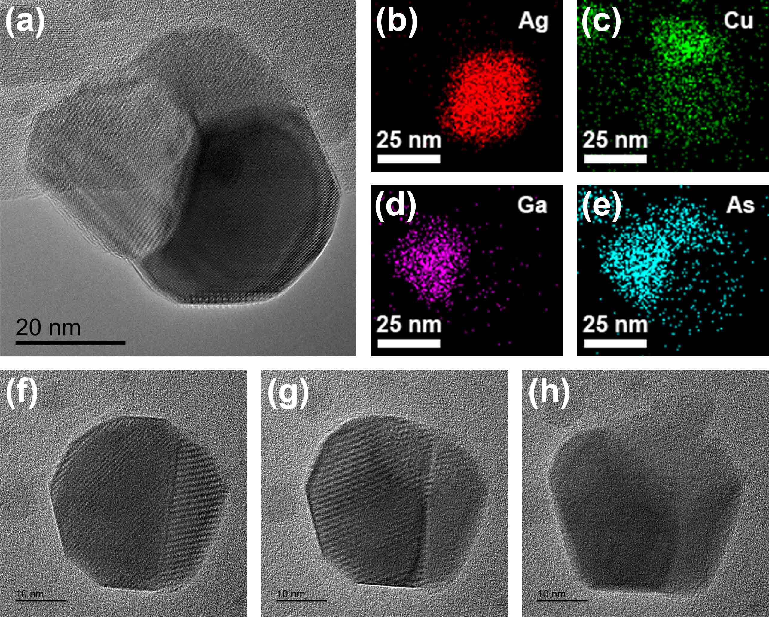
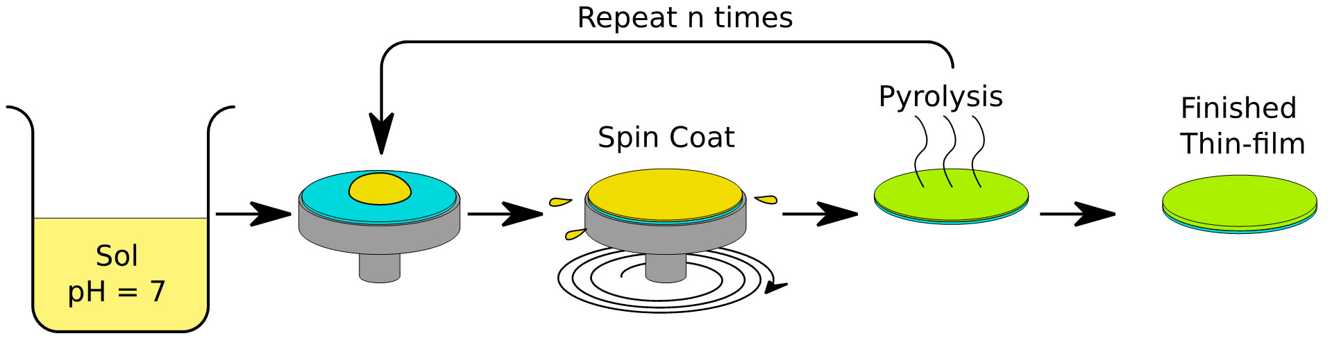
To save this page as a PDF, click this button and choose the PDF destination.

Physical Sciences Applications

14:00 - 16:00 Tuesday, 24th November, 2020

Meeting Room 2

Track Physical Sciences Applications

Presentation type Oral Presentation


14:00 - 14:15

92 Charge Discontinuity Induced Polarization Enhancement and Head-to-Head/Tail-to-Tail Polarization Configuration at Multiferroic/Ferroelectric BiFeO3/PbTiO3 Heterointerfaces

Dr Ying Liu1,2, Prof Yin-Lian Zhu1, Dr Yixiao Jiang1, Prof Yun-Long Tang1, prof Yu-Jia Wang1, Prof Xiu-Liang Ma1
11. Shenyang National Laboratory for Materials Science, Institute of Metal Research, Chinese Academy of Sciences, Shenyang, China. 22. Catalan Institute of Nanoscience and Nanotechnology (ICN2), Barcelona, Spain

Abstract Text

Functional oxide interfaces have received a great deal of attention owing to their intriguing physical properties induced by the interplay of lattice, orbital, charge, and spin degrees of freedom [1]. Ferroelectrics hold promise for sensors, transducers, and telecommunications [2]. With the demand of electronic devices scaling down, they take the form of nanoscale films. However, the polarizations in ultrathin ferroelectric films are usually reduced dramatically due to the depolarization field caused by incomplete charge screening at interfaces, hampering the integrations of ferroelectrics into electric devices [3]. Here, we designed and fabricated a ferroelectric/multiferroic PbTiO3/BiFeO3 system grown on SrRuO3/SrTiO3 (100) substrate, which exhibits discontinuities in both chemical valence and ferroelectric polarization across the interface. Aberration-corrected scanning transmission electron microscopy study reveals an 8% elongation of out-of-plane lattice spacing associated with 104%, 107%, and 39% increments of δTi, δO1, and δO2 in the PbTiO3 layer near the head-to-tail polarized interface, suggesting an over 70% enhancement of polarization compared with that of bulk PbTiO3. In addition to that in PbTiO3, polarization in the BiFeO3 is also remarkably enhanced. Electron energy loss spectrum (EELS) and X-ray photoelectron spectroscopy (XPS) investigations demonstrate the oxygen vacancy accumulation as well as the transfer of Fe3+ to Fe2+ at the interface. On the basis of the polar catastrophe model, FeO2/PbO interface is determined. First-principles calculation manifests that the oxygen vacancy at the interface plays a predominate role in inducing the local polarization enhancement [4].

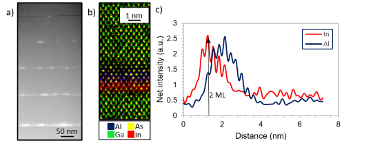
Besides the giant polarization enhancement at the BFO/PTO interface, both head-to-head positively charged and tail-to-tail negatively charged BFO/PTO heterointerfaces were successfully fabricated by controlling electric boundary conditions of the BFO/PTO film system. Aberration-corrected scanning transmission electron microscopic mapping reveals a head-to-head polarization configuration present at the BFO/PTO interface when the film was deposited directly on a SrTiO3 (100) substrate. The interfacial atomic structure is reconstructed, and the interfacial width is determined to be 5 ~ 6 unit cells. The polarization on both sides of the interface is remarkably enhanced. Atomic-scale structural and chemical element analyses exhibit that the reconstructed interface is rich in oxygen ions, which effectively compensates for the positive bound charges at the head-to-head polarized BFO/PTO interface. In contrast to the head-to-head polarization configuration, the tail-to-tail BFO/PTO interface (with TiO2/BiO termination) exhibits a perfect coherency, when SrRuO3 was introduced as a buffer layer on the substrates prior to the film growth. The width of this tail-to-tail interface is estimated to be 3 ~ 4 unit cells, and oxygen vacancies are supposed to screen the negative polarization bound charge. This study may facilitate the development of nanoscale ferroelectric devices by tailing the coupling of charge and lattice in oxide heteroepitaxy [5].

Uncaptioned visual

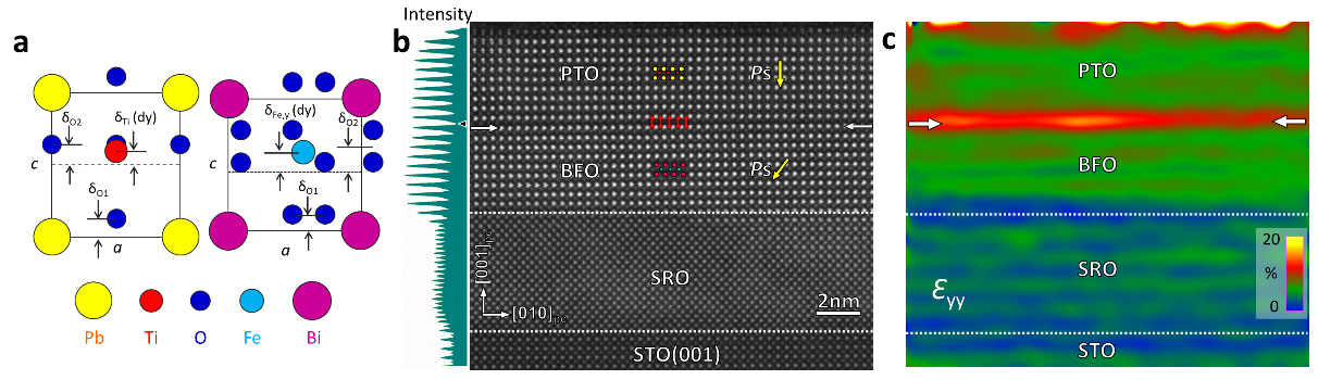
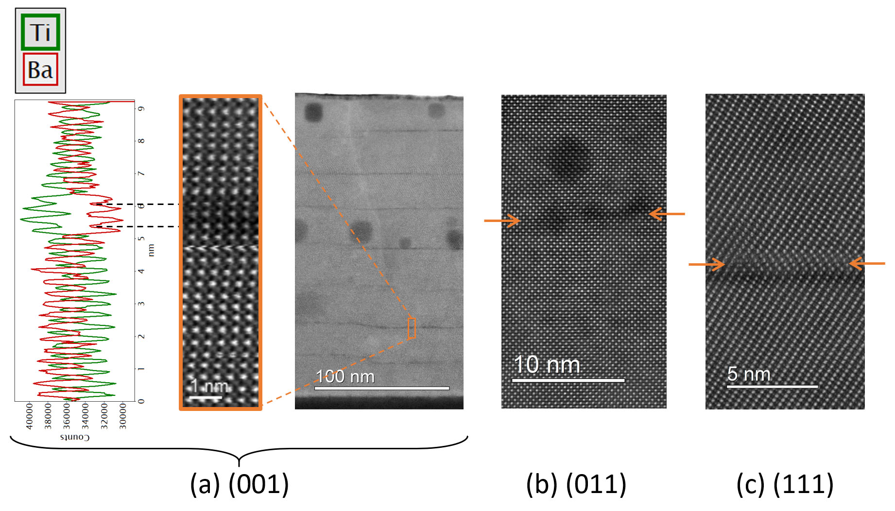
Figure 1 (a) Schematics of PTO and BFO crystallography structure; (b) A HAADF-STEM image of PTO/BFO thin film grown on SRO/STO (100) substrate; (c) Geometric Phase Analysis of out-of-plane lattice strain of the thin film.  

Uncaptioned visual

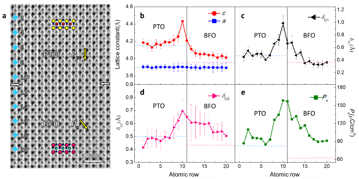
Figure 2 (a) An ABF-STEM image of the BFO/PTO interface; (b-e) lattice constants, O1, O2 displacements extracted from (a); (e) Calculated out-of-plane ferroelectric polarization of the BFO/PTO thin film.

Uncaptioned visual


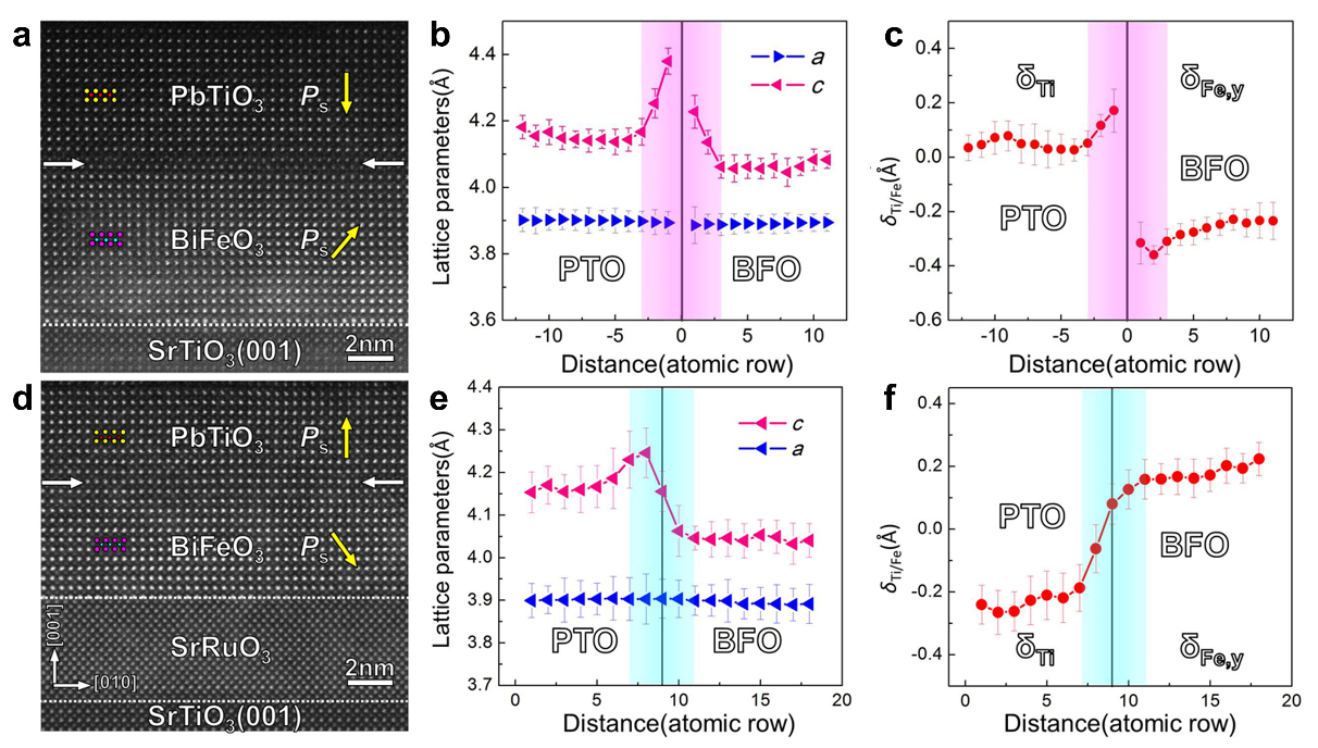
Figure 3 (a-c) A HAADF-STEM image, lattice parameters and Ti/Fe displacements of the head-to-head positively charged BFO/PTO interface; (d-f) A HAADF-STEM image, lattice parameters and Ti/Fe displacements of the tail-to-tail negatively charged BFO/PTO interface.


References

[1] H. Y. Hwang, et al. Nat. Mater. 11 (2012) p. 103 

[2] M. Dawber, et al. Rev. Mod. Phys. 77 (2005) p. 1083 

[3] C. L. Jia, et al. Nat. Mater. (2007) p. 64

[4] Y. Liu, et al. Nano Lett. 17 (2017) p. 3619 

[5] Y. Liu, et al. ACS Appl. Mater. Interfaces (2017) p. 25578 

[6] The authors gratefully acknowledge funding from National Natural Science Foundation of China (Nos. 51231007, 51571197, 51501194, and 51401212), National Basic Research Program of China (2014CB921002), and the Key Research Program of Frontier Sciences CAS (QYZDJ-SSW-JSC010).


14:15 - 14:30

238 Investigation of dynamic processes in Janus particle-seeded III-V semiconductor nanowires

Michael S. Seifner1,2, Markus Snellman2,3, Daniel Jacobsson1,2,4, Knut Deppert2,3, Maria E. Messing2,3, Kimberly A. Dick1,2,3
1Centre for Analysis and Synthesis, Lund University, Lund, Sweden. 2NanoLund, Lund University, Lund, Sweden. 3Solid State Physics, Lund University, Lund, Sweden. 4National Center for High Resolution Electron Microscopy, Lund University, Lund, Sweden

Abstract Text

The dynamic processes occurring during the nucleation and growth of III-V semiconductor nanowires seeded via two-phase Ag-Cu particles are in the focus of in situ transmission electron microscopy (TEM) investigations. For that purpose, particular attention is paid to the origin of the nucleation, the step-flow growth of bilayers forming the nanocrystal, the elemental distribution, and the epitaxial relations between the solid components.

A wide range of different metals promoting the anisotropic growth of III-V semiconductor nanostructures can be found in literature.[1] In general, metal seeds have the potential to alter the physical properties of a nanowire by triggering the formation of a metastable phase,[2] incorporating foreign atoms from the metal seed in the nanowire host lattice,[3] favouring growth in uncommon growth directions,[4] and transferring defects from the seed into the nanowire crystal.[5] Nevertheless, some of these processes, e.g. the formation of deep level traps in Si nanowires via the incorporation of atoms from the Au seed in the Si crystal,[6] are not desired and deteriorate the physical properties of a material. Therefore, the investigation of dynamic processes in crystal growth and the influence of synthesis parameters is of high importance for the semiconductor industry, which aims for tailoring the physical properties of a nanomaterial to be applicable in devices.

The mechanisms of metal-seeded nanowire growth performed in the gas phase can be divided into the vapour-liquid-solid (VLS) and the vapour-solid-solid (VSS) approaches, which describe the state of the present phases during growth conditions.[7] The state of the seed during the growth process is an important criterion for characterising the transport pathways of atomic species towards the growth front of a nanowire. However, there remain many open questions concerning the growth mechanism for both VLS and VSS growth of semiconductor nanowires and various parameters including the involved phases / elements and synthesis conditions have to be taken into account.

The growth of III-V semiconductor nanowires using solid Ag[8] and Cu[9] seeds is already reported in literature; however, Ag-Cu Janus particles and two-phase seed particles in general have not been considered as growth promoter so far. The motivation of this study is the potential introduction of additional possibilities for tuning nanowire properties by the controlled incorporation of defects using two-phase particles as growth seeds.

For that purpose, Ag-Cu Janus particles produced in a spark discharge generator are deposited on a SiNx-coated heating chip for in situ TEM investigations. Subsequently, the chip is transferred into an environmental TEM (ETEM) with the possibility to add metal-organic precursors. A detailed description of the used setup can be found elsewhere.[10] Chemical vapour deposition is performed at the heated area of the chip and the processes are traced by high-resolution bright-field imaging with aberration correction, electron diffraction, high-angle annular dark-field (HAADF) scanning transmission electron microscopy (STEM), and energy dispersive X-ray (EDX) measurements.

Initial experiments are focused on the behaviour of Ag-Cu particles under different conditions and atmospheres. Moreover, the influence of further elements of group III / V added to the binary system are investigated. The controlled switching between different morphologies of the seed particle is a major finding in this study. The elemental distribution at an early stage of GaAs nucleation is shown in Figure 1a-e and suggests enrichment of As in Cu. The origin of GaAs nucleation is mainly observed at the solid-solid interface of a Ag-Cu Janus particle, which is highlighted in Figure 1f-h. Representative frames of an in situ TEM movie acquired during the supply of arsine (AsH3) and trimethylgallium (TMGa) in the presence of a Ag-Cu Janus particle at elevated temperatures suggest the (f+g) formation of the GaAs nucleus at the triple phase boundary of the Janus particle and (h) a subsequent rearrangement of the components. Furthermore, first analyses point towards the possibility to transfer the solid-solid interface of the Janus particle into the nanowire crystal.


Uncaptioned visual

Figure 1. (a-e) STEM-EDX measurements on a structure obtained at an early stage of the nucleation process shown in (a) reveal the elemental distribution of (b) Ag, (c) Cu, (d) Ga, and (e) As. Enrichment of As in Cu is clearly visible in (c+e) suggesting the presence of a Cu-As alloy during nucleation. (f-h) The chronological steps of the nucleation process of GaAs nanowires using a Ag-Cu Janus particles as growth promoter are highlighted by representative frames of an in situ TEM movie. (f) shows a Janus particle with a Ag- (left) and Cu-rich part (right). (g) Nucleation at the triple phase boundary of the Janus particle is observed after the supply of both precursor species. (h) Rearrangement of the different phases occurs, once a GaAs nucleus is formed.


The conscious use of two-phase particles for metal-seeded nanowire growth is presented in this conference contribution. A deeper understanding of nucleation and growth of nanowires using two-phase solid seed particles is obtained and a novel approach for the controlled formation of defects in nanostructures to tailor the physical properties is introduced. This proof of concept for Janus particle-seeded nanowire growth has the potential to pave the way for a new approach to manipulate physical properties at the nanoscale in a controlled manner.[11]

References

[1] K. A. Dick and P. Caroff, Nanoscale 6 (2014), p. 3006.

[2] J. Tang et al, Nanoscale 9 (2017), p. 8113.

[3] M. S. Seifner et al, ACS Nano 13 (2019), p. 8047.

[4] E. C. Garnett et al, Advanced Materials 19 (2007), p. 2946.

[5] S. Barth et al, Nano Letters 11 (2011), p. 1550.

[6] E. Koren et al, Nano Letters 11 (2011), p. 2499.

[7] P. C. McIntyre and A. Fontcuberta i Morral, Materials Today Nano 9 (2020), p. 100058.

[8] A. T. Vogel et al, Nanotechnology 22 (2011), p. 015605.

[9] K. Hillerich et al, Journal of Crystal Growth 315 (2011), p. 134.

[10] C. Hetherington et al, Semiconductor Science and Technology 35 (2020), p. 034004.

[11] The authors gratefully acknowledge financial support from the Knut and Alice Wallenberg Foundation (KAW).


14:30 - 14:45

361 Transmission electron microscopy of interfaces between SrTiO3 substrates and BaTiO3 thin films with different crystallographic orientations

Inger-Emma Nylund, Trygve M. Ræder, Per Erik Vullum, Tor Grande
Norwegian University of Science and Technology (NTNU), Trondheim, Norway

Abstract Text

Transmission electron microscopy (TEM) was used to study interfaces in BaTiO3 thin films, deposited on (001), (011) and (111) oriented SrTiO3 substrates by aqueous chemical solution deposition (CSD). In particular, high-angle annular dark-field scanning TEM (HAADF-STEM) and electron energy-loss spectroscopy (EELS) was used to investigate the BaTiO3-SrTiO3 interface. Moreover, due to multiple CSD depositions, internal interfaces between each deposited layer in the BaTiOthin film were also observed and characterized by STEM-EELS.


BaTiO3 is a widely used material, e.g. in capacitors, due to its high dielectric constant, but it is also of interest for other applications due to the ferroelectric properties inherent to the material. Furthermore, CSD of thin films is attractive because it can produce high quality thin films at low cost and high scalability potential. In this study, the BaTiO3 thin films were grown on (001), (011) and (111) oriented SrTiO3 substrates. The CSD process shown in Fig. 1 was repeated eight times for each thin film, and the pyrolysis step included heating to 1000°C and keeping it at that temperature for 10 minutes. Due to the difference in thermal expansion coefficient between BaTiO3 and SrTiO3, a tensile in-plain strain is introduced in the films during cooling from 1000°C to room temperature. In-plane ferroelectric properties of the films were characterized by interdigitated electrodes [1].

Uncaptioned visual

Figure 1. Schematic showing the CSD procedure used to make BaTiO3 thin film. The process was repeated eight times (n=8).


The aim of this work has been to use TEM to investigate how the deposition method, including the high processing temperature, and the differently oriented substrates affect the thin film growth in terms of degree of texture, the Sr-Ba interdiffusion at the substrate-thin film interface, as well as formation of dislocations at the interface during relaxation. In addition, internal interfaces occurring due to the layered deposition technique were discovered and characterized.


The thin films grown on (001), and (011) substrates have a uniform thickness of 230±4 nm and 218±2 nm, whereas the thin film grown on (111) appears to have areas of uniform thickness, and some areas with a rough surface structure, resulting in a thickness of 220±27 nm. The thin films are not 100% dense, due to pores of varying size (Fig.2 (a) and (b)). Selected area diffraction reveals that the thin films grown on all the differently oriented substrates show a high degree of texture, and that they are relaxed, which is expected for film thicknesses in this range [2]. Periodically spaced edge dislocations are observed for all the three cases, and the Burgers’ vectors are determined to be mainly a<100>, a<110>, and a<111>, for the thin films grown on the (001), (011), and (111) oriented substrates, respectively. EELS performed across the substrate-thin film interface indicates a Sr-Ba interdiffusion length of about 10 unit cells, reflecting the high processing temperature. Lastly, internal interfaces between layers deposited one at the time by the CSD technique are found to be divided by thin interlayers (~1nm) that are significantly Ba-deficient, see Fig. 2. These internal interfaces are the surface of the thin film at each heating step, and Ba-deficiency can be explained by the volatility of Ba [3]. The (001) and (011) oriented thin films display no modifications of the crystal structure across these internal interfaces, whereas the (111) oriented thin film also exhibit internal interfaces with defects and twinning. In the (111) oriented thin film a grain that is twinned compared to the surrounding film is also observed. The high surface energy of the (111) plane compared to the (001) and (011) planes in BaTiO3 [4] may explain the appearance of twinning in the (111) thin film.

Uncaptioned visual

Figure 2. HAADF-STEM images of the three differently oriented thin films. (a) EELS is used to confirm that the internal interfaces (dark contrast bands in the STEM images) are Ba-deficient. Z-contrast is utilized to observe Ba-deficiency for the two other orientations, (011) (b) and (111) (c), indicated by orange arrows. Also visible is the twinning of the internal interface in (111) (c).


Using TEM to study these BaTiO3 thin films has shown that it is possible to grow high quality thin films by CSD, and that they are highly textured and relaxed by edge dislocations. The high processing temperature causes a relatively large Sr-Ba interdiffusion length at the substrate-thin film interface. Lastly, the orientation of the substrates affects the internal interfaces in the thin films. The crystal structure of the internal interfaces in the (001) and (011) oriented thin films remain unmodified, whereas crystal defects and twinning are observed at some of the internal interfaces in the (111) oriented thin film [5]. 

References

[1] T. M. Raeder et al., AIP Advances, 8 (2018), p. 105228

[2] T. Suzuki, Y. Nishi and M. Fujimoto, Philosophical Magazine A, 79 (1999), p. 2461

[3] R. Sažinas, M.-A. Einarsrud, T. Grande, J. Mater. Chem. A, 5 (2017), p. 5846

[4] M. Nakayama et al., J. Ceram. Soc. Jpn., 121 (2013), p. 611

[5] The Research Council of Norway is greatly thanked for financial support through the TOPPFORSK (250403/F20) and BORNIT (275139/F20) projects. The Research Council of Norway is further acknowledged for the support to the Norwegian Micro- and Nano-Fabrication Facility, NorFab, project number 245963/F50 and for the support to the Norwegian Center for Transmission Electron Microscopy, NORTEM (197405/F50).


14:45 - 15:00

600 Influence of thin AlAs capping layers on the structural and compositional properties of InAs QDs

Ms Nazaret Ruiz Marín1, Mr Daniel Fernández Reyes1, Ms Sara Flores Gallegos1, Ms Teresa Ben Fernández1, Mr Lazar Stanojevic2, Mr Alejandro Gallego Carro2, Ms Alicia Gonzalo2, Mr José María Ulloa2, Mr David González3
1Universidad de Cádiz, Puerto Real, Spain. 2Universidad Politécnica de Madrid, Madrid, Spain. 3Universidad de Cádiz, Cádiz, Spain

Abstract Text

SUMMARY

The structural features of the use of thin capping layers (CLs) of AlAs to implement in InAs quantum dot solar cells (QDSC) is investigated. On one hand, our results from EDX spectroscopy at the atomic scale contradict the hypothesis of a removal of the wetting layer (WL) during AlAs capping that should increase the open current voltage in QDSCs. Instead, we have observed an almost overlapping from the first monolayers (MLs) of the AlAs and InAs profiles that masks the contrast of the InAs WL at lower magnifications. On the other hand, the average QD size, areal density and In content, which have a clear interrelationship with the characteristics of the resulting WL, were determined by a combination of EDX, EELS and ADF measurements. The QDs show an almost linear increase of the In composition with the number of MLs of the AlAs layer following an Ostwald ripening-like behavior.

INTRODUCTION

Low dimensional nanostructures such as InAs QDs have been proposed as a means of implementing the intermediate band concept in QDSCs due to their discrete density of states and the maturity of the technology. However, for its success, several issues such as the thermal decoupling between the QDs and the conduction band of the WL needs to be overcome. A possible solution is the use of thin AlAs CL since it has been proposed that could reduce the WL effect because of the substitution of In by Al atoms1. In addition, AlAs should accumulate on top of the QDs, resulting in larger QD size and avoiding the In migration to the WL2. In this work, we have studied these effects using different thickness of AlAs CLs on InAs QDs by means of state-of-the-art structural and compositional TEM and STEM-related techniques. 

MATERIALS AND EXPERIMENTAL DETAILS

A sample consisting in 5 QD layers with 2.7 monolayers (MLs) of InAs on (100) n+ GaAs substrate was grown by solid source molecular beam epitaxy. The QD layers were capped respectively with different thin AlAs CLs (0, 1, 2, 3 or 5 ML) followed by 50 nm GaAs. Diffraction contrast (DC) TEM analyses were carried out in a FEI Talos F200X. Annular dark field (ADF)-STEM imaging, energy dispersive X-Ray spectroscopy (EDX) with ChemiSTEM technology and low-loss electron energy loss spectroscopy (EELS) analyses were performed simultaneously in a FEI Titan Cubed3 Themis. 

RESULTS AND DISCUSSION

Certainly, the analysis by DCTEM using chemical sensitive g200 DF conditions and ADF imaging (Fig. 1a) evidences a gradual contrast fading of the InAs WL as the thickness of AlAs CL increases being finally almost replaced by that of AlAs itself. It seems to point to the suggested progressive substitution of the In atoms in the WL by the deposited Al1. However, EDX analysis at the nanometer scale demonstrates that Al atoms do not substitute In atoms but there is no hard interaction between them. In fact, there is an In/Al distribution overlapping from the second monolayer of the WL that hides the presence of the WL when using DCTEM or ADF imaging techniques (Fig. 1c).


Uncaptioned visual


Figure 1. (a) ADF image of the 5 layers. The contrast of regions between QDs (WL) changes from brighter (without AlAs) to darker (5 ML of AlAs) respect to GaAs regions. (b) Atomic  resolution EDX map of the WL with 3 ML of AlAs. (c) Average EDX profiles of In and Al along the growth  direction of (b). Al signal is observed  from the 2nd InAs layer.


On the other hand, the size, composition and density of QDs are evaluated since they are key properties in the efficiency of QDSCs. First, a statistical study of the size of several dozens of QDs was carried out using color LUT ADF images where the criterion to size measurement were previously calibrated by comparing to EDX maps (Fig. 2 (a-c)). A significant increase of the QD heights with the AlAs thickness is found. Second, QD densities were estimated by combining the dot statistics with thickness measurements from low loss EELS maps. An inverse relationship is noticed between the average volume and the QD densities that points to a kind of Ostwald ripening process. The mean volume and density of the QDs together to measurements of the In content in the WL allowed us to calculate a statistical value of the average In content in QDs for each layer3. The estimated results show a linear increase of In content with the thickness of the AlAs layers. Indeed, In content values for individual QDs obtained by combining EDX measurements with EELS thickness maps are in agreement with the model (Fig. 2d). Nevertheless, the large increase of the In content of the QDs has a limited influence in the reduction of the WL because of the decay in the QD density by a ripening process.


Uncaptioned visual

Figure 2. ADF images (thermal LUT) corresponding to QDs without (a) and with (b) 5 ML of AlAs in the CL. (c) In and Al EDX map corresponding to a QD capped with 3 ML of AlAs. (d) Average In content of individual QDs (black squares) and the one obtained by the statistical model (red line) for the different layers.


References


1.           Tutu, F. K. et al. InAs/GaAs quantum dot solar cell with an AlAs cap layer. Appl. Phys. Lett. 102, 163907 (2013).

2.           Tsatsul’nikov, A. F. et al. Volmer-Weber and Stranski-Krastanov InAs-(Al,Ga)As quantum dots emitting at 1.3 μm. J. Appl. Phys. 88, 6272–6275 (2000).

3.           Gonzalez, D. et al. Quantitative analysis of the interplay between InAs quantum dots and wetting layer during the GaAs capping process. Nanotechnology 28, 425702 (2017).


15:00 - 15:15

604 Specific preparation and in situ electron holography experiments on working microelectronic nanodevices

Maria Brodovoi1,2, Frédéric Lorut1, Aurélien Masseboeuf2,3, Martin Hÿtch2, Christophe Gatel2,4
1STMicroelectronics, Crolles, France. 2CEMES – Centre National de la Recherche Scientifique (CNRS), Toulouse, France. 3Spintec – CNRS-CEA, Grenoble, France. 4Université Paul Sabatier, Toulouse, France

Abstract Text

The development of nanometer-scaled electronic devices such as Magnetic Random Access Memories (MRAM) [1], memristor [2] or Phase Change Memories (PCM) [3] requires a deeper understanding of their local properties, in particular when they are in operation. While electrical characterizations are used extensively to monitor and evaluate both the performance of devices and the quality of the layer stack, there is a lack of knowledge on how the electromagnetic fields are precisely mediated along the devices at the nanoscale level. Among Transmission Electron Microscopy (TEM) techniques, off-axis Electron Holography (EH) is a powerful interferometric method which allows the quantitative measurement of electric and magnetic fields not only within (internal fields) but also outside of the material/device (stray fields) [4-6]. In addition, other TEM methods such as high-resolution TEM, diffraction and electron spectroscopies can be combined for investigating structural, chemical and even thermal properties of the object on the same area of interest.

We developed a full process to select and prepare semiconducting nanodevices extracted from the production lines of STMicroelectronics for investigating their properties by in situ TEM. The originality of our approach is to quantitatively map the electric field and the electric charge distribution in building blocks from the industry (nanocapacitors, transistor, flash memory, phase change memory) using TEM when they are submitted to an external stimulus (voltage and current). The results will thus bring information on the local dielectric permittivity and capacitance for transistors and flash memories, the local electric resistivity and the thermal transition for phase change memories but also on the failure mechanisms of all these devices. These measurements by EH are correlated to complementary TEM methods as well as electrical measurement performed on wafers before device extraction for a full understanding of structural, chemical and electrical properties on a unique device at the nanometer scale.

Here we will present the different steps for extracting, preparing and in situ studying nanodevices of STMicroelectronics’ production lines using the state-of-the-art of EH experiments. In particular, we will detail the specific sample preparation to bring electrical stimuli to the device while ensuring its electrical connectivity and functionality after focused ion beam circuit modification. The final geometry of the electron transparent device is perfectly adapted for performing EH experiments under electrical stimuli.

This process has been applied on MIM (Metal-Insulator-Metal) matrix capacitors with common TiN bottom electrode, a thin Ta2O5 oxide dielectric and TiN top electrode stack. Samples are lifted-out from a fully processed wafer using Focused Ion Beam (FIB). Some preventive measures must be taken before the sample lift-out to ensure a proper charge evacuation during sample prepping, like depositing a thin protective layer of gold on the top surface of the region of interest. Besides, a pad opening is milled to connect the top surface to the grounded Si and the top electrode inputs are connected together to avoid electrostatic discharges (ESD) during the FIB-Edit. A representative thick trench of these capacitors is then withdrawn from the capacitor matrix and welded to an adapted TEM grid with Au pads which act as an electrical connection between the device and TEM holder for electrical biasing. The final thinning by FIB has been optimized in order to minimize the degradation of the device [7].

TEM experiments are carried out on the I2TEM-Toulouse microscope, an HF3300-C (Hitachi) TEM specially designed for in situ electron interferometry experiments. The microscope is equipped with a cold field-emission gun (CFEG) for optimal brightness, a double stage configuration and the latest generation of imaging aberration corrector (BCOR from CEOS) allowing for on and off-axis aberrations to be corrected on wide fields of view. The TEM studies run on working capacitors offer a complex understanding of the electrical behavior of the device. EH experiments enabled the quantification of the electric field across the insulator layer, as well as the inference of the charge density. The figure shows the amplitude image with isophase contours on a very large area (6 µm x 500 nm) including 3 nanocapacitors. The corresponding phase image presents only the electrostatic contribution with a bias of 1V after subtraction of the mean inner potential contribution using holograms acquired with 0V of bias. Some other post-biasing experiments were performed on the connected capacitors, like EDX analysis, which show a closed chemical composition of the failed regions. 

Our approach unlocks the visualization of the physical phenomena at the nm-scale on working nanodevices and will be applied on nanodevices of microelectronics industries (transistor, flash memory, phase change memory) as well as on recent developments in laboratories as spintronics devices.

Uncaptioned visual

MIM nanocapacitors observed by EH under a bias of 1V. From top to bottom: low magnification of the device connected to Au pads of the Si3N4 membrane, TEM image of the studied area, amplitude image with isophase contours showing the isopotential lines, phase image used for calculating the contours displayed on the amplitude image.


References

[1] J.S. Moodera, L.R. Kinder, T.M. Wong, and R. Meservey, Phys Rev Lett 74, 3273 (1995).

[2] D.B. Strukov, G.S. Snider, D.R. Stewart, and R.S. Williams, Nature 453, 80 (2008).

[3] S. Raoux, G.W. Burr, M.J. Breitwisch, C.T. Rettner, Y.C. Chen, R.M. Shelby, M. Salinga, D. Krebs, S.H. Chen, H.L. Lung, and C.H. Lam, IBM J. Res. Dev. 52, 465 (2008).

[4] A. Tonomura, Rev. Mod. Phys. 59, 639–669 (1987).

[5] P. A. Midgley and R. E. Dunin-Borkowski, Nat. Mater. 8, 271–280 (2009).

[6] J. F. Einsle, C. Gatel, A. Masseboeuf, R. Cours, M. A. Bashir, M. Gubbins, R. M. Bowman, and E. Snoeck,  Nano Res. 8, 1241–1249 (2015).

[7] A. N. Campbell, K. A. Peterson, D. M. Fleetwood and J. M. Soden, 1997 IEEE International Reliability Physics Symposium Proceedings. 35th Annual, Denver, CO, USA, 1997, pp. 72-81.


15:15 - 15:30

888 Correlation between the particle and nanowire composition during in-situ InGaAs nanowire growth in an environmental TEM

Robin Sjökvist1,2, Daniel Jacobsson1,2, Axel R. Persson1,2, Marcus Tornberg1,3, Carina B. Maliakkal1,2, Reine Wallenberg1,2, Kimberly A. Dick1,2,3
1NanoLund, Lund University, Lund, Sweden. 2nCHREM and CAS, Lund University, Lund, Sweden. 3Solid State Physics, Lund University, Lund, Sweden

Abstract Text

The goal of this study is to give insight into the growth of ternary InGaAs semiconductor nanowires, to enable nanowire growth models that fit more closely to reality. Specifically, the composition in the seed particle is correlated with the resulting nanowire composition during growth within an environmental transmission electron microscope (ETEM) connected to a metal organic vapor phase epitaxy (MOVPE) system. The composition is measured by in-situ high-temperature x-ray energy dispersive spectroscopy (XEDS).

For the past couple of decades, III-V semiconductor nanowires, e.g. GaAs and InAs, have been studied extensively for their optical and electronic properties [1]. These nanowires can be grown by supplying heat and growth material in the form of precursor molecules, to a metallic nanoparticle (often Au) within an MOVPE system. The precursor molecules supply the growth species into the nanoparticles, which catalyze the growth of the one-dimensional nanowires. The incorporation of more than one element from either group III or group V in the periodic table will lead to the formation of a ternary material, e.g. InGaAs, where the resulting properties depend (non-linearly) on the properties of the two ingoing III-V binaries, GaAs and InAs in this case. This enables tailoring of material properties, such as the bandgap, to make the nanowires fit specific applications. The actual growth of nanowires is often regarded as a black box, where the combination of input parameters (temperature, V/III ratio, total pressure, etc.) results in either successful growth or not, but the mechanisms actually taking place during the growth are unknown. The reason is that, in conventional MOVPE, most analysis can only be carried out after the growth is completed, when the surrounding conditions are very different compared to during growth. However, due to recent developments, several aspects of the growth are now being unraveled by utilizing ETEMs, wherein the growth process can be observed in real time. For example, the composition within Au-Ga-As catalysts has been analyzed extensively during the growth of Au catalyzed, binary, GaAs nanowires [2]. When growing ternary nanowires, the addition of another element makes the growth even more complex and difficult to control. Here the interplay between the two materials from the same group within the catalyst particle is an interesting and important factor that will determine the final composition in the nanowire. However, this correlation has so far not been analyzed experimentally. Due to the lack of experimental data, the spread in predictions from theoretical models is large [3], [4].

In this project, a Hitachi HF-3300S ETEM [5] is used to study the growth of ternary InxGa1-xAs semiconductor nanowires in-situ, to find out how the composition within the catalyst particle affects the composition in the nanowire. 30 nm Au particles are used as catalyst nanoparticles. The ETEM is connected to an MOVPE system, which supplies the precursor molecules required for the growth. It is also equipped with a Cs aberration image corrector (CEOS “B-COR”), a cold field emission gun and a OneView IS (Gatan) camera, to enable up to 25 fps 4k-by-4k (or 300 fps binned to 512-by-512) pixels recordings with atomic resolution at elevated pressures during growth. The Au-In-Ga-As composition is measured via in-situ high-temperature XEDS, where spectra are recorded of both the particle and the subsequently formed nanowire, see Figure 1. To be able to follow the particle during growth, the spectra are recorded using a condensed beam in parallel mode. A particle spectrum is recorded by focusing on the tip of the particle facing away from the nanowire (orange in Figure 1). Similarly, the beam is then focused on the area just below the particle (purple in Figure 1) to get a spectrum from the wire grown from this particle composition. Movies of the growth are recorded so that the growth rate can be measured, and to determine the number of layers grown during a measurement period. The resulting correlation between the particle and wire compositions is compared to predictions made from existing theoretical models. Based on this comparison, the reliability of the current models, and suggestions to improve them, are discussed [6].

Uncaptioned visual

Figure 1: XEDS spectra recorded for the nanoparticle, as well as the growing nanowire close to the interface. The Si signal is originating from other parts of the TEM. The micrograph is extracted from a movie of a growing nanowire.


References

[1] H. J. Joyce et al., IEEE J. Sel. Top. Quantum Electron. vol. 17 no. 4 (2011), p. 766-778.

[2] C. B. Maliakkal et al., Nat. Commun. vol. 10 no. 1 (2019), p. 1-9.

[3] E. D. Leshchenko et al., Cryst. Eng. Comm. vol. 20 no. 12 (2018), p. 1649-1655.

[4] A. S. Ameruddin et al., Nanoscale vol. 7 no. 39 (2015), p. 16266-16272.

[5] C. Hetherington et al., Semicond. Sci. Technol. vol. 35 no. 3 (2020), p. 034004-034013

[6] We acknowledge Erik Mårtensson, Martin Ek Rosén, Crispin Hetherington, Krishna Kumar and Michael Seifner for valuable discussions, and Sebastian Lehmann for valuable discussions and for assisting in particle deposition. We also acknowledge vetenskapsrådet (VR) and the Knut and Alice Wallenberg Foundation (KAW) for funding this project.


15:30 - 15:45

1042 Real-time observation of remote doping in core-shell GaAs nanowires using off-axis electron holography

Postdoc Ganapathi Prabhu Sai Balasubramanian1, PhD student Elizaveta Lebedkina2, Postdoc Nebile Isik Goktasb3, Professor and Chair Ray LaPierre3, Seniorforsker Elizaveta Semenova2, Associate Professor Marco Beleggia1, Forsker Elisabetta Fiordaliso1
1DTU Nanolab, Technical University of Denmark, Kongens Lyngby, Denmark. 2DTU Fotonik, Technical University of Denmark, Kongens Lyngby, Denmark. 3Department of Engineering Physics, McMaster University, Hamilton, Canada

Abstract Text

The aim of this work is to demonstrate the capability of off-axis electron holography in measuring real-time changes in dopant profiles across core-shell GaAs nanowires (NWs), carried out by in-situ annealing inside a TEM and assisted by the electron beam, through in-situ measurements of electrostatic potential at a spatial resolution of few nm.

Semiconductor NWs are powerful building blocks of nanoelectronic and optoelectronic devices. For controlling the electronic properties of the NWs the doping needs to be assessed at high enough spatial resolution. Most dopant assessment techniques like Raman spectroscopy, photoluminescence, secondary ion mass spectroscopy, do not have enough spatial resolution or are not sensitive solely to active dopants. Off-axis electron holography is a TEM technique where electrons passing through the specimen and vacuum interfere to produce a pattern that is sensitive to phase changes suffered by the electrons. Since the phase of the electron wave passing through the specimen is dependent on local variations in electrostatic potential, this technique is a direct technique for visualizing active dopants and potential profiles at atomic to nanoscale. In this work we focus on doping assessments carried out using medium resolution off-axis electron holography.

Our samples are GaAs NWs with undoped core and doped shell (p-doped or n-doped) and GaAs undoped NWs surrounded by a layer of C (acceptor in GaAs), as illustrated in Figure 1. We anneal these samples from room temperature to 700 °C in vacuum, inside a TEM, and acquire off-axis electron holograms as a function of T. Holographic measurements on GaAs NWs with undoped core and C doped shell acquired at room temperature show that the core is not at the geometric center of the NW. Moreover, the built-in potential between the core and the shell is found to be lower on the side where the core is closer to the shell. This result could be due to different dimensions of the depletion layers and charge density at the opposite i-p junctions, resulting in different values of built-in potentials. Line scans of electrostatic potential across the NW as function of temperature are shown in Figure 2. We observe changes in the profile of electrostatic potential across the NW at temperature of 400 °C and above, indicating a remote doping from the doped shell to the core. We have verified separately that As evaporation is not significantly affecting our results.   

At the moment, we are gathering more data from a similar sample where the p-type dopant is Be instead of C. We are also looking at undoped nanowires surrounded by a C layer. Moreover, we are also going to investigate the remote doping from a n-type shell (Te) to the intrinsic core of GaAs NWs.

In conclusion, we demonstrate that remote doping in the TEM is possible and that off-axis electron holography is a powerful technique in revealing real-time changes of dopant profiles across various type of junctions in semiconductor NWs.

We acknowledge financial support from Villum Experiment Programme. We also thank DTU Nanolab for supporting this work.

Uncaptioned visual

Figure 1. Schematic showing the cross-section of two types of nanowire samples


Uncaptioned visual

Figure 2. Electron holography data at different T for GaAs nanowire with undoped core and C-doped shell


References


15:45 - 16:00

1149 Point Defects Influence on the Structural and Electronic Properties of ß-(AlxGa1-x)2O3

Dr. Adrian Chmielewski1, Sarah Deng2, Parivash Moradifar1, Leixin Miao1, Kleyser Agueda Lopez1, Dr. Yuewei Zhang3, Akhil Mauze3, Dr. James Speck3, Dr. Wolfgang Windl2, Dr. Nasim Alem1
1Pennsylvania State University, University Park, USA. 2Ohio State University, Columbus, USA. 3University of California Santa Barbara, Santa Barbara, USA

Abstract Text

Beta-phase gallium oxide ß-Ga2O3 semiconductor is a very promising material for power electronics devices due to its large band gap (4.8 eV) and an expected high breakdown voltage (8 MV.cm-1). The addition of Al into ß-Ga2O3 leading to a ß-(AlxGa1-x)2O3 alloy enhances the electronic properties of this semiconductor enabling the design of many different semiconductor heterostructures such as modulation doped field effect transistors (MODFETs) [1]. However, the link between growth-induced defects and their potential impact on the structural and electronic properties of ß-(AlxGa1-x)2O3 alloys remains to be explored. 


In this study we report direct observations of various point defects in ß-(Al0.2Ga0.8)2O3/ß-Ga2Ointerface and their role in the electronic properties using high resolution scanning/transmission (HR-S/TEM) imaging and electron energy loss spectroscopy (EELS). In addition, this study further investigates the distribution and coordination of Al, as well as Al and Ga interstitials in ß-(Al0.2Ga0.8)2O3/ß-Ga2Oepitaxial film and their impact on the electronic structure of the film.

Figure 1 shows a HR-STEM image of the ß-(Al0.2Ga0.8)2O3/ß-Ga2Ointerface. Interestingly the Al/Ga interstitials (highlighted by blue circle in the top insert) are mainly present in the ß-(Al0.2Ga0.8)2O3 film whereas the ß-Ga2O3 is almost defect free. Moreover, we will show that the number of interstitials increases at the interface.  In order to describe the effect of these defects on the electronic properties, we have performed EELS scan across the interface to probe the volume plasmon of Ga. Using the Drude model, we can deduce the free electron density across the ß-(Al0.2Ga0.8)2O3/ß-Ga2O3 interface. We will show that the electron density is increased by ~ 2e-.nm-3 at the interface and is induced by the higher density of Al/Ga interstitials at the interface.


To get insight at atomic scale of the Al/Ga interstitials within the ß-(Al0.2Ga0.8)2O3 film, density functional theory (DFT) calculations have been carried out within the Vienna Ab initio Simulation Package (VASP) [2]. Two initial ß-(Al0.2Ga0.8)2O3 structures were generated and studied. We considered both Ga and Al interstitial in our calculations. Figure 1.b shows the initial structure of ß-(Al0.2Ga0.8)2O3/ß-Ga2Oin [001] projection with a Ga interstitial (blue circle) placed initially in the tetrahedral site. The Ga interstitial will induce distortion in the ß-(Al0.2Ga0.8)2O3 matrix that will push some of the nearest Ga neighbors creating new interstitials as highlighted by the red circle in the relaxed structure in Figure 1.c. These new interstitials act as deep-level donor whereas distortions caused by Al interstitials creates a shallow donor state. This report provides a better understanding, at the nanoscale, of the effect of point defects on the electronic structure of ß-(AlxGa1-x)2O3 alloy that is meaningful for the development of future gallium-oxide based applications. 


Uncaptioned visual

Figure 1. (a) HR-STEM image of the ß-(Al0.2Ga0.8)2O3/ß-Ga2Ointerface in the [001] projection. Yellow circles are highlighting the Al and/or Ga interstitial as shown in the zoom-in image on the insert. The defects are mainly in the ß-(Al0.2Ga0.8)2O3 film whereas the substrate is almost defect free. (b) Initial structure of ß-(Al0.2Ga0.8)2O3/ß-Ga2Oin [001] projection with a Ga interstitial (blue circle) placed initially in the tetrahedral site. (c) Relaxed structure of the Ga- interstitial in ß-(Al0.2Ga0.8)2O3 in [001] projection. Ga interstitials induce distortion of certain nearest neighbors creating new interstitials atoms that are pushed from their initial positions as highlighted by a red circle.  


References

[1] Y. Zhang et al., 112, 233503 (2018)

[2] G. Kresse and J. Furthmüller, 54, 10 (1996), p. 11169-11186