16:00 - 16:05
Misfit-layered compounds (MLCs) are stacks of two different layered materials, which have a lattice mismatch at least in one direction [1]. MLCs based on chalcogenides are composed of a metal chalcogenide (MX) and a transition-metal chalcogenide (TX2) and tend to form tubular structures due to the misfit stress and the elimination of dangling bonds upon seaming. Applying the chemical vapour transport (CVT) technique, MLC-nanotubes (NTs) can be synthesized with a high yield [2]. MLC-NTs are promising for applications, e.g. in the field of thermoelectricity, due to the complementary properties of the two layered compounds [3]. An improvement of the synthesis process of MLC-NTs allows alloying the compounds forming quaternary structures starting from LaS-TaS2 [4]. This work focusses on the electron microscopy study of the family of quaternary (La,Y)S-TaS2 nanotubes [5].
Using aberration-corrected transmission electron microscopy (TEM), we analysed the NTs by high-resolution (scanning) (S)TEM, electron diffraction (ED), energy-dispersive X-ray spectroscopy (EDX) and electron energy-loss spectroscopy (EELS) revealing their structure and composition. The synthesis of NTs was successful for the whole range of Y percentages between 0 to 100% with the NT yield being largest at 10% (global) and 80%. The two HAADF STEM images (Figure 1) reveal the layered misfit structure of one layer of TaS2 (TX2) and two layers of (La,Y)S (MX). While for pure NTs (0 and 100% Y) the layers were found to share the same orientation, quaternary structures often show two sets at different orientation that appear at double periodicity (alternating contrast of stacks in Figure 1b).
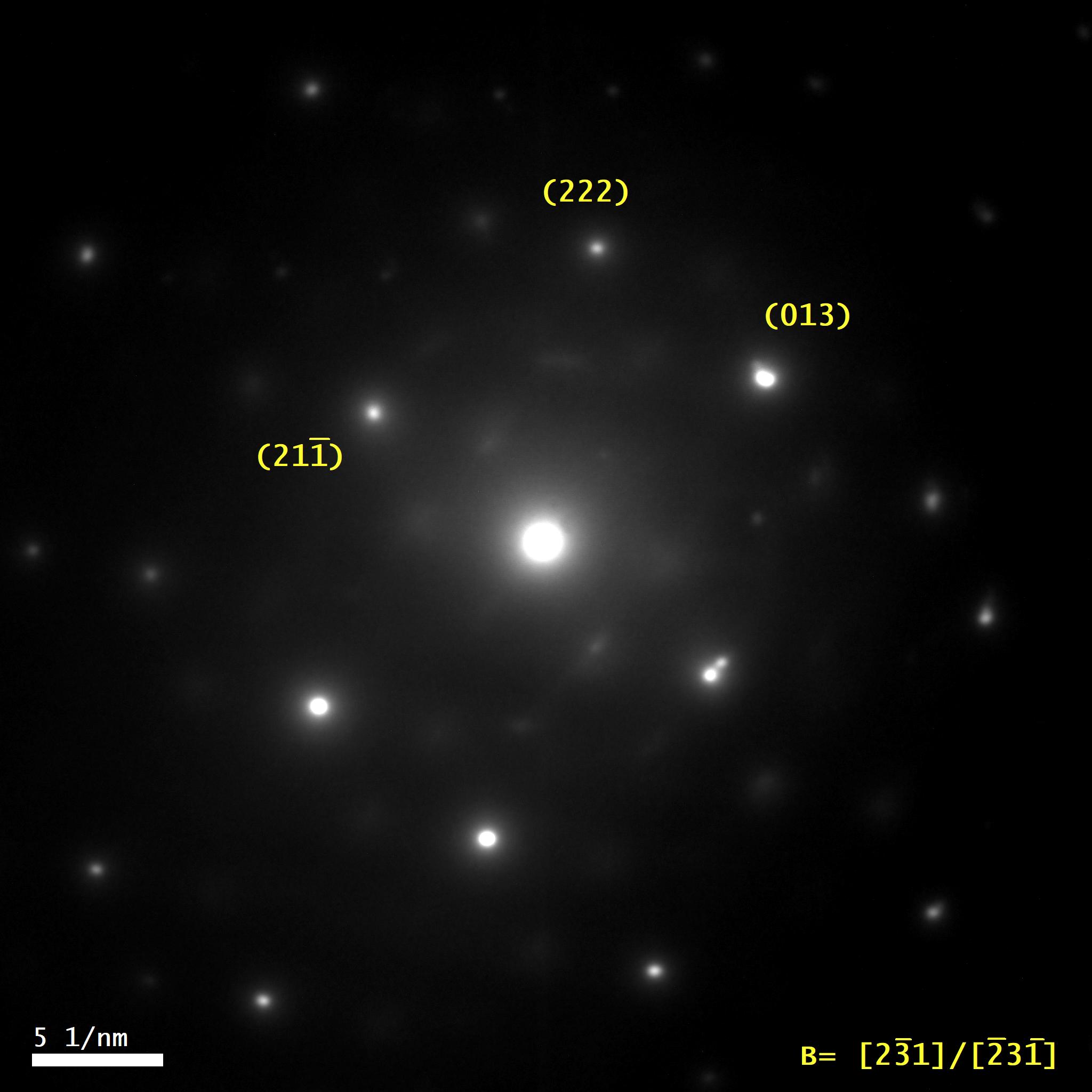
These predominant orientations are confirmed by ED results (Figure 1c), where 2x4 and 2x6 sets of reflections stemming from the (La,Y)S and TaS2 sublattices, rotated by 30º, are observed. ED also indicates a decreasing stack periodicity from 1.15 nm (0% Y) to 1.09 nm (100% Y) as well as a slightly shrinking lattice parameter of the (La,Y)S sublattice being in agreement when considering values of LaS and YS.
EELS measurements suggest a homogeneous and in-phase substitution of La by Y as shown by the spectrum imaging map in Figure 2a. The intensity of the Y-L edge at 2080 eV clearly increases with respect to the Ta edge for increasing Y content (Figure 2b). STEM-EDX results indicate a stoichiometric composition of the NTs for Y percentages >20% while only a reduced content of <5% Y is observed for an intended composition of La:Y 90:10 suggesting increased stability of Y-doped LaTaS NTs.
In conclusion, we were able to deduce the dependence of the structure and properties of the NTs on the Y content by in-depth EM analysis [5,6].
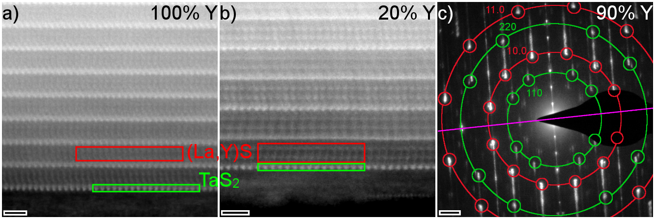
Figure 1: STEM images of different (La,Y)S-TaS2 NTs with (a) 100% Y showing a similar appearance of the layers and (b) 20% Y showing alternating contrast of the layers along c. (c) ED pattern of a 90% Y- NT showing 2x4 sets of 110 and 220 (La,Y)S reflections (green) and 2x6 sets of 10.0 and 11.0 reflections of TaS2 (red). Tube axis is indicated by the purple line and scale bars are (a,b) 1 nm and (c) 1 nm-1.
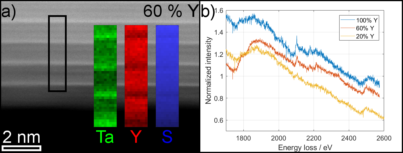
Figure 2: (a) EELS spectrum image for NT with 60% of Y revealing the spatial separation of Ta and Y in the MX and TX2 layers. (b) Comparison of EELS spectra normalized before Y-L edge shows increasing intensity of Y-L edge (2080 eV) with Y content as well as S-K (2472 eV) and Ta-M edge (1735 eV).
[1] GA Wiegers, Prog Solid State Ch 24 (1996), 1–139.
[2] G Radovsky et al.. Angew Chem Int Edit 50(2011), 12316–12320.
[3] M Serra, R Arenal, R Tenne, Nanoscale 11 (2019), 8073-8090.
[4] G Radovsky et al., J Mater Chem C 4 (2016), 89–98.
[5] S Hettler, M.B. Sreedhara, M. Serra, S. Sudarson Sekhar, R. Popovitz-Biro, I. Pinkas, A. N. Enyashin, R. Tenne and R. Arenal, submitted.
[6] Research supported by the Spanish MINECO (MAT2016-79776-P, AEI/FEDER, EU), Government of Aragon through project DGA E13_17R (FEDER, EU) and European Union H2020 program “ESTEEM3” (823717).
16:10 - 16:15
Whether grown by CVD, exfoliated, after transfer or in a final device, 2D materials are typically supported by a substrate. In these cases, cross sectional samples offer the most direct way of investigating the number of layers, morphology and crystal structure. TEM examination in cross-section requires thinning and polishing. In this case, FIB can be used to prepare these structures after growth [1] or after patterning/contacting [2-3]. Surface damage introduced during FIB preparation, can often be limited to the range of few nm, either by protective layers [4-5] or adjusted milling procedures [6-7]. This is sufficient in all cases where the surface atoms are not of explicit interest. For 2D materials the surface atoms constitute the region of interest, and thus hardly any surface damage during preparation can be tolerated. This work shows, that carbon coating prior to FIB preparation, limits surface damage to a level where investigations of the surface atoms of the original sample is possible. Exfoliated and chemical vapor deposited MoS2 multi and monolayers on a pure gold surface are examined using (scanning) transmission electron microscopy, and it is demonstrated that evaporated carbon protects these structures [8].
Figure 1: (a) Optical micrograph of exfoliated MoS2 showing color contrast indicating monolayer MoS2, prior to application of protective coatings, with indication of the region where the lamellae was extracted. (b) Cross sectional STEM-HAADF image of the surface showing monolayer MoS2. (c) Vertically averaged image intensity from the blue box in the STEM-HAADF image above with comparison of expected position of molybdenum atoms and peaks in image intensity. (d) Cross sectional STEM-HAADF image of bilayer CVD grown MoS2. (e) Vertically averaged image intensity from the blue and red box in the STEM-HAADF image above, shown as blue and red curves respectively, with comparison of image intensity and the expected position of the sulfur and molybdenum atoms.
[1] Ang-Yu Lu et al., Nature Nanotechnology 12 (2017), p. 744.
[2] Yang Wang et al., Nature 568 (2019), p. 70
[3] Lei Wang et al., Science 342 (2013), p. 614
[4] YC Park et al., Journal of Microscopy 255 (2014), p. 180.
[5] S. Rubanov and P.R. Munroe 225 Material Letters (2003), p. 180.
[6] M. Baram and W.D Kaplan 232 Journal of Mircroscopy (2008), p 395.
[7] N. I. Kato, 53 Journal of Electron Microscopy p. 451.
[8] A. B. A, T. B., A. S. and T. W. H acknowledge support from the Danish National Research Foundation Center of Excellence for Nanostructured Graphene (CNG) (project DNRF103)
16:15 - 16:20
Continuously diminishing fossil fuel resources, environmental concerns and changing geo-political scenario have incentivised the search of alternative energy resources and technologies. In this changing scenario, hydrogen may evolve as a new energy currency. It has been realised that single point solution to this energy problem is not quite achievable due to the limitation arising out of resources, climatic conditions etc. Judicious selection of energy technologies and its exploitation in its most efficient form is the way forward. Vanadium alloys have attracted attention in the recent past due to its high-temperature strength, low activation, fast decay characteristics, non-magnetic properties. In addition to that vanadium alloys may be used in metal hydride batteries due to its ability to absorb hydrogen [1]. However, very little is known about its phase transformation behaviour and microstructural evolution and the kinetics of hydrogen absorption-desorption is strongly dependent on the alloying elements present in the alloy. Apart from the formation of hard and brittle intermetallic phases, V-alloys might undergo phase separation followed by omega(ω)-transformation in the system [2]. Last decade has observed an upsurge in research activities in development, processing and characterisation of vanadium alloys with a view to apply this material in fusion reactors and in metal-hydride batteries. In course of this development, mostly two alloys have received most attention and those are V-4Ti-4Cr and V-4Ti-4W [3]. Both the alloys are in the vanadium rich corner of the phase diagram. As cast alloys are single phase BCC in structure. It has been observed that the alloys possess high strength up to high temperature. However, limited creep properties, He-embrittlement coupled with processing difficulties of these alloys serves as the motivation to better understand the physical metallurgy of such V-alloys at the atomic scale.
Elemental V and Ti (both >99.7% purity) in the form of rods were procured from Alfa Aesar and routine X-Ray Diffraction (XRD) patterns were recorded from them for cross-verification. Thermodynamic calculations, especially the semi-empirical approach put forth by Andries Miedema, were performed on the V-Ti binary system. The data when fed to his model generated several curves on an Enthalpy versus mole fraction plot which in turn led us to judiciously select compositional variants of the V-Ti system to be vacuum arc-melted. The Miedema plot suggests that this binary system has quite a large maxima coming from the elastic contribution to enthalpy which shoots off steeply and attains its peak at equi-atomic composition which in turn suggests possible phase separation event.
Three Ten gram buttons of binary V-Ti alloy were prepared through vacuum arc melting in an argon back-filled chamber, composition being: V-10%Ti, V-15%Ti and V-30%Ti (expressed by weight). The buttons were re-melted 5-7 times each so as to attain uniform chemical composition throughout its volume. SEM-EDS chemical mapping showed uniform composition variation of V and Ti in all the alloys, although with minute oxygen pick-up. Additionally, pure vanadium was heated by pulsed laser in a controlled oxygen atmosphere to study the effect of oxygen dissolution. Transition metals, having high affinity towards oxygen, leads to modification of the surface microstructure as have been confirmed from diffraction-contrast and phase-contrast microscopy. Due to oxygen incorporation a new phase is nucleated at the surface which is plate like in morphology. The diffraction pattern from the plate like phase indicates that it is related to the cubic phase. However, there is elongation along the c-axis and contraction along the a- and b-axes. Our First principles DFT calculation also indicates that oxygen incorporation introduces strain in the lattice and in order to accommodate the strain the BCC structure transforms to Tetragonal structure. Furthermore, the as-melted V-Ti alloys have been characterized by X-Ray diffraction studies in a high-resolution diffractometer using Cu-target. The I vs. 2θ plots hence generated from the cast alloys, when stacked vertically above the plot of pure vanadium revealed a consistent left-ward shift of the fundamental peaks coming from the bcc alloy. This implies that upon alloying vanadium with increasing Ti-content, lattice parameter of the disordered BCC unit cell also went up by small fractions of an angstrom unit. But as it turns out from extensive TEM investigations, such straight forward interpretation is perhaps not true and the shift in the peak positions arise due to convolution of several effects at the sub-microstructural level. Ex-situ TEM analysis reveal extensive diffused scattering in all ZAP’s except along <111> with dove-tail streaking and spot-splitting in V-15%Ti alloy. In the imaging setup, nano-precipitates of titanium, whisker-like morphology, localized phase-separation events could be spotted. In-situ heating the V-10%Ti specimen up to 950°C followed by cooling within the scope has revealed co-existence of two kinds of nano-sized precipitates in the V-rich cubic matrix. There seems to be a yet unexplored shallow energy landscape over which the V-Ti binary system likes to hop from one local minima to the other. Microstructure, phases and its stability will be presented in detail.
The authors would like to take this opportunity to thank SERB-DST for support through grant EMR/2016/007512.
Figure 1: A micro-beam diffraction pattern from V-15%Ti as-cast alloy showing extensive diffuse scattering along with satellite spotting
Figure 2: Corresponding BF diffraction-contrast image revealing highly anisotropic whisker-like morphology.
[1] E. Akiba & H. Iba, “Hydrogen absorption by Laves phase related BCC solid solution” Intermetollics 6 (1998) 461-470.
[2] Chanchal Ghosh, Joysurya Basu, Divakar Ramachandran, E. Mohandas, “Phase separation and ω-transformation in binary V-Ti and ternary V-Ti-Cr alloys” Acta Materialia 121, 2016, 310-324.
[3] E. E. Bloom, R. W. Conn, J. W. Davis, R. E. Golo, R. little, K. R. Schultz, D. L. Smith and F. W. Wiffen, “Low activation materials for fusion applications” Journal of Nuclear Materials 122 & 123 (1984) 17-26.
16:25 - 16:30
Many important optical technologies rely on objects or features much smaller than the diffraction limit of light, consequently, optical-based microscopies and spectroscopies have insufficient spatial resolution to interrogate the nanoworld.
In this talk, I will introduce cathodoluminescence (CL) – the emission of photons from a material excited by an electron beam—showing how we can use CL detectors such as the Monarc® system to analyze optical emissions of individual nanostructures thereby revealing emission probability, wavelength distribution and polarization state of the emitted light at a spatial resolution better than 20 nm.
Having the ability to study optical properties at deep sub-wavelength resolution really opens the door to answering a wide range of important questions from basic science problems such as how light and matter interact at the nanoscale to industrial solutions such as failure analysis of LED devices and displays, making cathodoluminescence—and the Monarc detector—an impressively powerful characterization tool for the nanoworld.
16:30 - 16:35
Fig. 1a Projection of the crystal structure along [100]. b: ) HRTEM with overlaid model of disorder of Al atoms (blue) within the pentagonal pattern. Large pentagons correspond to Co-containing columns.
High-resolution TEM, STEM, and X-ray diffraction experiments on orthorhombic o-Al13Co4, a quasicrystal approximant, confirmed the symmetry of space group Pmn21, reported by the first study of this crystal structure [1,2]. HRTEM and HRSTEM images revealed a structural arrangement with strong local violations of translational symmetry, in particular by aluminum positions located on the mirror plane, see Fig. 1a,b.
In crystallography, there is a constant struggle to understand the real structural organization of complex intermetallic compounds. The compound o-Al13Co4 has attracted attention of several research groups because of its unusual physical and chemical properties. In addition, it is an efficient and highly selective hydrogenation catalyst for alkynes.
Single crystal of o-Al13Co4 was grown by the Czochralski technique. For TEM investigations focused ion beam (FIB) lift-out lamella were prepared with cuts parallel to (100) plane. The lamellae were further treated by the milder argon ion polishing at lower energies in order to obtain even thinner samples.
In order to verify the assumption of local atomic disorder, the study was continued by means of high-resolution transmission electron microscopy. A comparison with the structure model, obtained from the X-ray diffraction data, shows that the main contrast features of the high-resolution TEM (HRTEM) micrograph along [100] direction are created by vertex- and edge-connected Co pentagons. Within the large pentagon, a smaller-sized pentagon shows up, formed exclusively by aluminum atoms. In the center of each of these double-pentagons, a column consisting of cobalt and aluminum atoms is situated. The aluminum atoms within the pentagons are disordered. Bonding interactions between the three-dimensional framework and three-atomic groups Co-Al-Co located in the cavities of the latter in combination with large distances between the cages and cage caps are one possible reason for the extended disorder. The local twinning in different directions together with stacking faults is another possible origin of the experimentally observed crystallographic features [3].
[1] J. Grin, U. Burkhardt, M. Ellner, K. Peters. Crystal structure of orthorhombic Co4Al13. (1994) J. Alloy. Compd. 206, 243-247.
[2] J. Grin, U. Burkhardt, M. Ellner and K. Peters. Refinement of the Fe4Al13 structure and its relationship to the quasihomological homeotypical structures. (1994) Z. Kristall. 209, 479-487.
[3] P. Simon, I. Zelenina, R. Ramlau, W. Carrillo-Cabrera, U. Burkhardt, P. Gille, Y. Grin. Structural organization of the intermetallic catalyst o-Al13Co4. (2020) J. Alloy. Compd. 804, 153363.
16:35 - 16:40
A Pb(Zr0.52Ti0.48)O3–LaNiO3–Si (PZT/LNO/Si) composition and LNO thin films are synthesized using chemical solution deposition and studied by transmission electron microscopy. It is shown that LNO films actually has polycrystalline, multiphase and porous structure. Special features of LNO film structure are observed in samples annealed at temperatures of 550°C to 800°C.
Thin film heterostructures based on lead zirconate titanate (Pb(ZrxTi1 – x)O3) is a key component in different integrated ferroelectric devices [1, 2]. Lanthanum nickelate LaNiO3, with its pseudocubic perovskite structure and a lattice constant similar to that of PZT, is especially promising as an electrode material for such systems. Of particular interest is the ability to apply PZT/LNO/Si thin film composites as a part of a single process, such as chemical deposition from a solution [3]. Despite a fairly large number of publications devoted to the study of the electrical properties of the compositions, the structure of LNO electrodes has not been studied sufficiently [4, 5].
PZT/LNO/Si and LNO/Si compositions were prepared by chemical solution deposition. To form an LNO film, a precursor was applied layer by layer with drying and crystallization of each sublayer. The annealing temperature for the LNO layer in the PZT/LNO/Si compositions was 650℃. To form a PZT layer, precursor sublayers were deposited onto the LNO layer with annealing of the whole volume of the film at 650℃. To reveal the evolution of this structure during thermal treatment, LNO/Si compositions were annealed at temperatures T = 550, 650, and 800℃.
The grain structure, defects and local chemical and phase heterogeneity of the films were studied by transmission electron microscopy (TEM), high resolution electron microscopy (HREM), transmission scanning electron microscopy with z-contrast using a high-angle annular dark-field detector (HAADF STEM), electron diffraction, and EDX analysis (SuperX EDS system) in a FEI OSIRIS microscope (200 kV). TEM sample preparation was accomplished using a focused ion beam in a FEI Scios Dual Beam microscope.
It was shown, that the lead zirconate-titanate layer in t PZT/LNO/Si crystallizes heterogeneously from the substrate with the formation of a columnar perovskite phase (fig.1, a, b), however, the width of the columnar grains is 2-4 times less than that formed on a traditional platinum electrode [3]. The LNO layer is characterized by a fine-grained, porous structure.
Figure 1. Structure of compositions: a) BF TEM image of PZT/LNO/Si; b) SAED pattern of PZT; c,d) EDX mapping of LNO film; e) HRTEM image and corresponding FFT (f, g) of Ni3O4 grain
The evolution of the LNO structure during crystallization at T = 550 - 800 ºС is studied. It was found that the layering and porosity of the LNO structure are already manifested at T = 550 ºС. A further increase in temperature leads to the enlargement of grains from units of nanometers at T = 550 ºС up to 40 nm at T = 800 ºС, coagulation of pores and the formation of crack-like defects.
In the LNO layer, chemical and phase inhomogeneity were visualized for the first time at all stages of crystallization in the temperature range 550 - 800 ºС. The Ni3O4 (С2/m) and La2O3 (С2/m) phases are localized at the interfaces of the sublayers, and LaNiO3 (𝑃𝑚 ̅3𝑚) and La2Ni2O5 (С2/m) are located in their volume.
Despite the chemical and phase inhomogeneity, it was shown, that the electrical properties of such structures are close to the level of that formed on a platinum electrode [6].
[1] N. Setter, D. Damjanovic, L. Eng, G. Fox, S. Gevorgian, S. Hong, A. Kingon, et.al. J. Appl. Phys. 100, 051606 (2006).
[2] K. A. Vorotilov and A. S. Sigov, Phys. Solid State 54, 894 (2012).
[3] Zhigalina O.M., Atanova A.V., Khmelenin D.N., Kotova N.M., Seregin D.S., Vorotilov K.A., Crystallography Reports, 64 (6), p. 955–961 (2019).
[4] Z. Duan, Y. Cui, Z. Yang, K. Li, Y. Wan, Z. Lu, X. Xie, and J. Zhang, Ceram. Int. 44, 695 (2018).
[5] R. A. C. Amoresi, A. A. Felix, G. M. M. M. Lustosa, G. Gasparotto, A. Z. Sim s, and M. A. Zaghete, Ceram. Int. 42, 16242 (2016).
[6] This work is supported by the Ministry of Science and Higher Education within the State assignment FSRC “Crystallography and Photonics” RAS in the field of structural studies, the Russian Foundation for Basic Research (project No. 19-29-03058) in the field of synthesis of materials. The TEM study was performed using the equipment of the Shared Research Centre of the FSRC “Crystallography and Photonics” of RAS.
16:40 - 16:45
Gold-catalyzed III-V nanowires are grown epitaxially on microfabricated silicon microheaters in an environmental transmission electron microscope (ETEM). The study contributes to the fundamental understanding of crystal growth at nanoscale as well as the fabrication of future microdevices. The study includes both design, fabrication and characterization of microheaters integrated into a silicon on insulator (SOI) chip suitable for specialized ETEM holders. The setup is used for in situ nucleation and growth studies of gold-catalyzed III-V nanowires at different growth parameters on the silicon microheaters, which also work as substrate with a (111) crystal orientation.
Microheaters have previously been used for epitaxial growth of silicon nanowires [1]. Observing nanowires bridging from one microheater to another in situ TEM has resulted in unique studies of contact formation [2] and electrical characterization of single nanowires [3] resulting in nanowire based microdevices. The setup has also led to important fundamental results for nanowire growth measuring the surface tension of gold-catalyzed silicon nanowires [4]. The present study extends the previous observations with an extra dimension by studying gold-catalyzed III-V nanowire growth live in a unique ETEM with a purpose built gas handling system for metal-organic vapor deposition [5].
Silicon microheaters have been fabricated based on previous designs [6]. For silicon nanowires, the growth rate can be used to determine the temperature profile of the microheaters [6], but using more complex compositions such as III-V nanowires, other methods are used to determine the temperature profile for the microheaters including simulations with COMSOL Multiphysics®. Au-nanoparticles are introduced as catalyst particles using aerosol deposition. A good contact between the Au-nanoparticles and the silicon microheaters is important to get epitaxial growth. This is encouraged by annealing the microheaters on a hot plate in a nitrogen atmosphere right after gold deposition. Another important interface besides that of Au-catalyst and Si-substrate is the contact between the catalyst and the surrounding precursor gases. An oxide layer is formed on the surface of the catalyst and removing this is a part of the nucleation studies. Once the nanowires are growing, the suspended nanowire growth is investigated including the growth of crystal phase heterostructures. By changing gas flows, the crystal structure of the GaAs nanowire can be deliberately tuned from hexagonal wurtzite to cubic zincblende [7].
Microheaters prepared as described above are loaded into the ETEM. Applying a current to the device lead to resistive heating of the microheaters (figure 1a). The eutectic point of gold and silicon is found, when the gold particle forms a liquid alloy with the silicon substrate (figure 1b). As an AuSi liquid is formed and oxide has been removed from the catalyst surface, epitaxial growth is achieved (figure 1c), which is being confirmed by diffraction patterns (figure 1d-e). The epitaxial growth is used to study the effect of changing gas flows on crystal structure as control of the changing crystal structure can allow for formation of crystal phase heterostructure (Figure 2).
In conclusion, the present study investigates the growth of gold-catalyzed III-V nanowires on resistive heated microfabricated Si(111) cantilevers. It demonstrates different growth behaviors of the suspended nanowires by changing growth parameters [8].
Figure 1. Silicon microheaters integrated into a silicon on insulator chip hanging into vacuum (a). Applying a current will heat up the microheaters forming a liquid AuSi alloy. TEM images of AuSi alloy achieved at temperatures above the eutectic point (b) and an epitaxially growing nanowire (c). The epitaxial growth is verified by diffraction patterns (d) of both silicon microheater and GaAs nanowire (e).
Figure 2. Nanowire growing at different applied gas flows from one video sequence going from wurtzite (a) structure to introducing sections with zincblende structure (b). The snapshots are taken as the nanowire grows.
[1] K Mølhave et al, Small 4 (2008), p. 1741–6
[2] S B Alam et al, Nano Lett. 15 (2015), p. 6535–41
[3] C Kallesøe et al, Nano Lett. 12 (2012), p. 2965–70
[4] F Panciera et al, Nat. Commun. 7 (2016), pp. 12271
[5] C Hetherington et al, Semicond. Sci. Technol 35 (2020), pp. 34004
[6] C Kallesøe et al, Small 6 (2010), p. 2058–64
[7] D Jacobsson et al, Nature 531 (2016), p. 317–22
[8] We acknowledge financial support from DTU Nanolab, DTU Fotonik, the Knut and Alice Wallenberg Foundation (KAW), the Swedish Research Council (VR), and the Swedish Foundation for Strategic Research (SSF).
16:45 - 16:50
Point and extended defects -as well as their interaction with dopants- directly influence semiconductor properties hence, identifying different defect-types and understanding their formation and evolution is crucial. ZnO is a wide and direct band-gap semiconductor with a potential for a variety of next generation solid-state devices, however, the doping asymmetry -where only n-type conductivity can be accomplished- hinders the realization of ZnO applications. Nitrogen (N), has been considered as one of the most promising candidates for p-type doping in ZnO, however, the results obtained so far are quite contradictory and reliable p-type doping is still challenging. Furthermore, N-doped ZnO has also attracted fundamental interest since it exhibits a strikingly different behavior in terms of defect evolution, in comparison to other dopants. In particular, an exceptional thermal stability of vacancy-clusters has been reported, as well as nonlinear thermal evolution trends. However, the defect formation mechanism is not yet understood and atomically-resolved investigations are still pending in order to elucidate the role of N in defect evolution in ZnO.
This study provides a thorough comprehensive STEM-EELS investigation on the atomic scale, conducted for the first time, in order to elucidate the nitrogen behavior as a dopant in ZnO-based structures. In this respect, N-implanted ZnO single crystals were initially studied, to investigate the fundamentals regarding formation and thermal evolution of the N-induced defects [1]. The study continued to novel semiconductor alloys (ZnO)1−x(GaN)x (ZOGN), that are strong candidates for bandgap engineering [2], [3], [4], [5]. This system is of particular interest, since its bandgap energy is reduced in comparison to its binary compounds due to a strong band bowing effect, and can be tailored from the UV-range into the visible part of the spectrum, making ZOGN ideal for photovoltaic and solar water-splitting applications.
In our study, taking advantage of the possibility to use multiple detectors simultaneously, a direct correlation of the atomic structure to chemical information and bonding-type gave valuable insight into the elemental and bonding distribution on the atomic scale and its correlation to different defect-types. In this respect, (Scanning) Transmission Electron Microscopy ((S)TEM) was employed, combined with Electron Energy-Loss Spectroscopy (EELS) and Energy-Dispersive X-ray spectroscopy (EDX). STEM-imaging was conducted using simultaneously high-angle annular dark field (HAADF), annular dark field (ADF) and annular bright field (ABF) detectors, providing complementary views of the same defected region, through different mechanisms of the electron beam-specimen interactions. Low-loss EELS was employed for band gap measurements of the alloys and for the sample thickness evaluation. A time-resolved electron-beam irradiation experiment was also performed in order to modify in-situ a defected area, while simultaneously recording EELS spectra. Geometric Phase Analysis (GPA) was performed on high resolution (S)TEM images to extract lattice phase maps and for the nanoscale localization of strained regions. All investigations were conducted on an FEI Titan G2 60-300 kV equipped with a CEOS DCOR probe-corrector, monochromator and Super-X EDX detectors.
This study elucidates the behavior of nitrogen into ZnO and ZOGN host matrix and proposes a model describing the evolution of N-related defects. EELS showed direct evidence for the formation of N2 molecules, supporting previous reports on the low stability of N substitution on O sites (NO), thus limiting p-type doping. Vacancy (VZn) -clusters were found to be stabilized by N2-trapping, resulting in an exceptional thermal stability compared to the situation with other dopants, and leading to a suppression of Vzn-Zni recombination. The highly mobile Zn interstitials preferentially condense on the basal planes forming interstitial-type extended defects. The dominant extended defects were the energetically favorable basal stacking faults of I1-type terminated by stacking mismatched boundaries or Frank-Shockley dislocations, which again provide energetically favorable sites for N2-trapping as a way to reduce local strain fields. The same trend was observed in ZOGN alloys, where thermally-induced nano-sized voids (VZn+Ga) filled with molecular nitrogen (N2) were formed along grain boundaries. The voids reached an equilibrium shape defined by the energetically favorable facets, mainly on the semi-polar planes and the O-terminated internal polar plane. This study revealed that the N-N bonding is an alternative path for nitrogen after annealing of ZOGN alloys, in addition to the increase in the Ga-N bonds that reduce the total energy of the system. Despite this re-arrangement of N-bonds, no phase separation phenomena were observed (ZnO vs. GaN) indicating that the previously reported bandgap of the system is the result of a homogeneous ZOGN alloy and not an average of a mixture of different phases [6].
Figure 1. (a) ADF-STEM intensity map across a nano-sized vacancy-cluster in N-implanted ZnO and the corresponding (b) relative thickness map and (c) N-K intensity EELS map. (d) ADF-STEM image showing a faceted vacancy-cluster along grain boundaries in ZOGN alloys. (e) Comparison of monochromated EELS spectra revealing molecular nitrogen N2 being trapped at the vacancy-clusters.
[1] C. Bazioti et al., J. Phys. Chem. Lett. 10 (2019), 4725.
[2] C. Bazioti et al., Phys.Chem.Chem.Phys. Communication 22 (2020), 3779.
[3] V. S. Olsen et al., Phys. Rev. B 100 (2019), 165201.
[4] V. S. Olsen et al., Physica Status Solidi B 256 (2019), 1800529.
[5] V. S. Olsen et al., Semicond. Sci. Technol. 34(7pp) (2019), 015001.
[6] The authors gratefully acknowledge funding from the Research Council of Norway for support to the Norwegian Center for Transmission Electron Microscopy (NORTEM) (no. 197405/F50), the top-tier research project FUNDAMeNT (no. 251131), the Norwegian Micro and Nano- Fabrication Facility (NorFab) (no. 245963/F50) and the SALIENT project (no.239895).