To save this page as a PDF, click this button and choose the PDF destination.

Physical Sciences Applications

09:00 - 12:00 Thursday, 26th November, 2020

Meeting Room 2

Track Physical Sciences Applications

Presentation type Oral Presentation


09:00 - 09:15

192 Quantifying ordering phenomena in lanthanum barium ferrate at the atomic scale

Judith Lammer1, Christian Berger2, Stefan Löffler3, Daniel Knez1, Paolo Longo4, Edith Bucher2, Gerald Kothleitner1, Andreas Egger2, Rotraut Merkle5, Werner Sitte2, Joachim Maier5, Werner Grogger1
1Institute of Electron Microscopy and Nanoanalysis (FELMI), Graz University of Technology & Graz Centre for Electron Microscopy (ZFE), Graz, Austria. 2Chair of Physical Chemistry, Montanuniversitaet Leoben, Leoben, Austria. 3University Service Centre for Transmission Electron Microscopy (USTEM), TU Wien, Vienna, Austria. 4Gatan Inc., Pleasanton, USA. 5Max Planck Institute for Solid State Research, Stuttgart, Germany

Abstract Text

Within this abstract we present a high-resolution chemical analysis of the second order Ruddlesden-Popper phase Ba1.1La1.9Fe2O7 using EDX and EELS in STEM, as well as simulations for quantifying the lanthanum and barium concentration on each atom column.

Lanthanum barium ferrates have auspicious properties as triple conducting oxides (proton-, oxygen ion- and electron-conducting) and therefore are promising new materials for future applications in protonic ceramic fuel cells, electrolyser cells or membranes for hydrogen separation [1]. However, mass and charge transport as well as defect chemistry are only partially understood at this point. These properties are influenced by the crystal structure and the distribution of the elements within this structure.

In this work, we show an element analysis of the second order Ruddlesden-Popper phase Ba1.1La1.9Fe2O7. In addition to characterizing the crystal structure over a large material volume by X-ray diffraction (XRD), we used scanning transmission electron microscopy (STEM) in combination with electron energy loss spectrometry (EELS) and energy-dispersive X-ray spectrometry (EDX) to locally analyse the elemental distribution down to the atomic scale via high-resolution elemental maps.

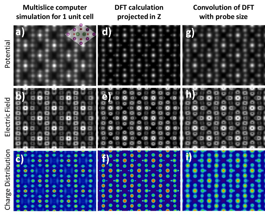
Both La and Ba occupy the A-sites within the crystal. Our experiments show that La favours the 9-fold coordination sites in the rock salt layer, whereas Ba prefers the 12-fold coordination sites within the perovskite block (fig. 1a). Moreover, we recognised fluctuations in the Ba/La distribution on each atom column within both rock salt and perovskite layers (fig. 1b). In order to quantify the EELS spectrum images, one needs to be aware of signal contributions stemming from neighbouring atom columns, which may have serious influence due to the in-zone-axis conditions during data acquisition. Hence we simulated the La and Ba EELS signal using inelastic multislice calculations based on Slater-type orbitals and analysed the contributions coming from either the investigated atom column (on-axis signal) or the neighbouring atom columns (off-axis signal). In doing so, we are able to estimate the off-axis contributions to the experimentally determined signal and therefore quantify the La and Ba concentrations on each atom column. A previous work on the nominal material Ba1La2Fe2O7 shows similar behaviour when it comes to the preferred site of La and Ba in the rock salt and the perovskite layers, respectively [2]. We additionally revealed that (in terms of crystal structure) equivalent atom columns within either the rock salt layer or the perovskite layer do not exhibit distinct La/Ba ratios but a broad variation in concentration.

The cation diffusion within the crystallites and the new insights on cation ordering in Ba1.1La1.9Fe2O7 further contribute to the understanding of mass and charge transport properties in order to systematically design new materials for intermediate temperature protonic ceramic fuel cells [3].


Uncaptioned visual

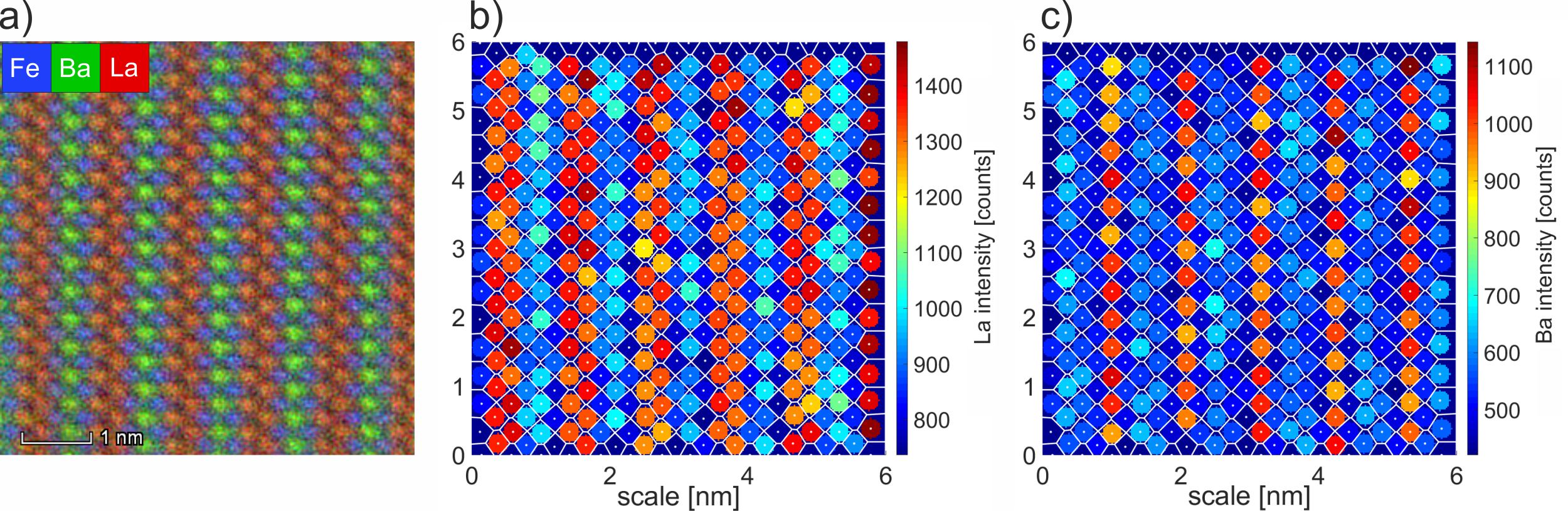
Figure 1: a) The EDX elemental map depicts the distribution of La, Ba and Fe in the second order Ruddlesden-Popper phase Ba1.1La1.9Fe2O7 in [100] orientation. b) and c) La and Ba intensity maps evaluated per atom column illustrate the intensity variations on equivalent atom columns. 

References

[1] R Zohourian et al, Advanced Functional Materials 28 (2018), 1801241

[2] NNM Gurusinghe et al, Materials Research Bulletin 48 (2013), p. 3537–3544

[3] The support of the Austrian Research Promotion Agency FFG (No. 853538), the Klima- und Energiefonds within the program "Energieforschung (e!MISSION)", the European Union Horizon 2020 programme (grant 823717–ESTEEM3) and the Austrian Science Fund FWF (No. I4309-N36) is gratefully acknowledged.


09:15 - 09:30

259 Comprehension of gassing mechanism of Ni-rich positive electrode material for lithium-ion batteries through surface analysis by high energy resolution STEM-EELS

Angelica Laurita1, Pierre-Etienne Cabelguen2, Liang Zhu2, Dominique Guyomard1, Nicolas Dupré1, Philippe Moreau1
1Université de Nantes, CNRS, Institut des Matériaux Jean Rouxel, IMN, Nantes, France. 2Umicore, Rechargeable Battery Mat, Brussels, Belgium

Abstract Text


The electrification of vehicles presently relies on lithium ion batteries using layered oxides of nickel, manganese and cobalt (NMC) with high Ni content as positive electrode materials. Nevertheless, it has been demonstrated that these materials suffer from gassing issues decreasing cycle life and causing safety problems [1,2]. Moreover, nickel-rich NMCs are affected by critical instability during all the manufacturing steps (synthesis, handling, electrode preparation). A deep comprehension of the pristine material properties and of its behaviour during electrode preparation and electrochemical cycling is thus fundamental from the industries’ point of view.

In this context a systematic study of the surface reactivity of NMC811 (Li[Ni0.8Mn0.1Co0.1]O2) was conducted using a multi-analytical approach in which transmission electron microscopy plays an essential role. A new TEM/STEM Themis Z G3 (Thermo Fisher Scientific) equipped with a double camera GIF spectrometer, was, in fact, recently installed in the Jean Rouxel Institute of Materials of Nantes (France). Electron Energy Loss Spectroscopy (EELS) was in particular exploited in order to give a complete description of the surface of the material.

The direct detection camera (Gatan K2 Summit) allowed the acquisition of EELS spectra in STEM mode with both high energy and spatial resolution. This enables a good multi-elemental chemistry mapping quantification (at low energy dispersions) as well as the accurate analysis of the fine structures of the Ni L23 -edges thanks to the use of an excited monochromator. Moreover, the use of a vacuum transfer sample holder insured the observation of samples without any contact with the ambient atmosphere. The samples were in fact transferred directly to the microscope from the Argon glove box where they were stored, preventing any sort of reaction of the material with air and thus allowing the proper analysis of the material in its initial state.

In this way it was possible to look at the surface modifications and to compare them to the bulk structure by means of the multiple linear least square (MLLS) fitting; the thickness of the surface modified layer was then determined for all the samples, proving the high reactivity of the material surface in the ambient atmosphere. The Ni L3-edge changes in fact between the surface and the bulk of the material, indicating its oxidation state’s evolution after 5 days of exposition in air. The reduced Ni was found for about the first 15 nm of the surface. Correspondingly, the disappearance of the oxygen pre-edge was observed.

On the other hand, the analysis of the same powder transferred directly from the glove box revealed a similar behaviour of the Ni L-edge (Figure 1) in the first 6 nm of surface only; a slight change in the shape of the oxygen K-pre-edge was also observed, indicating that a gradual but not yet completed evolution of the material surface.

Uncaptioned visual

Figure 1: Evolution of Ni L-edge in the pristine NMC 811 powder

Similarly, the calculation of the ratio between the Ni L3/L2-edges was performed on the entire EELS spectrum image allowing the valence mapping of the material after the comparison with proper references.

Moreover, through the calculation of the second derivative of the EELS spectra, a quantification of all the transition metals was performed. In fact, it has to be considered that the small quantity of Mn and Co in the material doesn’t usually allow the correct quantification of these species, since the corresponding intensity signal is too low and often confused into the background. For this reason, changes in the surface composition of this materials have rarely been deduced by EELS spectra at this level of precision.

In addition to primary particle analysed above, FIB lamella were also produced on secondary particles (made of these primary particles) actually used by our industrial partner. First results on these closer to application samples will be presented so that we can demonstrate how the observed phenomena on primary particles translate at a larger scale.

To conclude, EELS Spectrum Images were analysed in order to obtain qualitative and quantitative information about the surface of NMC811, essential to the good comprehension of its reactivity and gassing behaviour. EELS was used for the determination of both the valence state, coordination and quantity of all the transition metals as well as for the qualitative identification of surface modifications in particular aging conditions.


References

[1] Berkes, B. B. et al,  60 (2015), 64.

[2] Mantia, F. L. et al, 156 (2009), A823.


09:30 - 09:45

644 Sodiation of different-stacked SnS2 by In-Situ Transmission Electron Microscopy

Mr. Zhongtao Ma1, Dr. Zhenpeng Yao2,3, Prof. Yingchun Cheng4, Dr. Xuyang Zhang4, Prof. Bingkun Guo1, Prof. Yingchun Lyu1, Prof. Peng Wang1, Prof. Qianqian Li1, Prof. Hongtao Wang5, Prof. Anmin Nie1,6, Prof. Alán Aspuru-Guzik2,3
1Materials Genome Institute, Shanghai University, Shanghai, China. 2Department of Chemistry and Chemical Biology, Harvard University, Cambridge, Massachusetts, USA. 3Department of Chemistry and Department of Computer Science, University of Toronto, Toronto, Ontario, Canada. 4Key Laboratory of Flexible Electronics & Institute of Advanced Materials, Jiangsu National Synergetic Innovation Center for Advanced Materials, Nanjing Tech University, Nanjing, China. 5Center for X-mechanics, Zhejiang University, Hangzhou, China. 6Center for High Pressure Science, State Key Laboratory of Metastable Materials Science and Technology, Yanshan University, Qinhuangdao, China

Abstract Text

Summary: In-situ TEM is used to investigate the phase transition pathway and ionic diffusion of SnS2 with different structural symmetry upon (de)sodiation by nanobattery preparation. Intermediate semi-stable phases such as AA1 NaSnS2 for trigonal SnS2 and AB1 NaSnS2 for hexagonal SnS2, are observed after sodium ions fully occupy all Oh sites, and following alloying/conversion processes are entirely elucidated for the first time. The results allow us to identify the entire cycle reaction mechanism. The in-situ TEM results are supported by results from DFT, XPS and XRD.

Introduction: Layered two-dimensional (2D) transition metal sulfides like tin sulfides (SnS2) with remarkable electrochemical capacity are promising candidates as anodes in sodium-ion batteries [1]. There are two common polytypes of SnS2: the trigonal P-3m1 SnS2 [2] and the hexagonal P63mc SnS2 [3]. However, the influence of structural symmetry of SnS2 on the structural evolution requires further investigation, and an in-situ study can uncover the microstructural development of two types of SnS2 fundamentally. 

Methods: To determine the structural evolution, the (de)sodiation reaction was conducted inside the TEM chamber by the nanobattery setup on a homemade holder developed at Center for X-Mechanics, Zhejiang University. It is equipped with a compact four-degree freedom (positioning in X, Y, Z-directions plus self-rotation) nano-manipulator and in-situ electrical potential functions. SnS2 nanoparticles were held with semicircular carbon film fixed on Au rod. Sodium metal acted as the counter electrode that can move with the nano-manipulator. The sodiation reaction occurs when we apply a negative bias of ca. 2.5 V between the two electrodes, and the desodiation reaction would be triggered when the bias is positive. 

Results and Conclusion: Trigonal and hexagonal SnS2 with distinct Sn, S arrangement are synthesized by two different hydrothermal routes. The intercalation processes of these two SnS2 polytypes were characterized by time-resolved selected area electron diffraction (SAED) (Figure 1). The results show that semi-stable intermediate phases (NaxSnS2 (0<x<1) and NaySnS2 (0<y<1)) form before initially all the Oh sites are occupied by Na-ions and trigonal/hexagonal SnS2 phase completely transforms to AA1/AB1 NaSnS2. The results were supported by DFT calculations.

Keeping the negative bias of the holder at ca. 2.5 V and with the progress of sodiation process, crystal structures of the samples are generally rearranged and finally collapsed when sodium strikes a critical amount. The SnS, β-Sn, amorphous Na2S, Na15Sn4, polycrystal Na2S form in sequence during sodiation [4]. When the opposite bias is applied, the sodium is extracted from the sample, and the Na15Sn4 dealloy to Na metal and SnS phase. The Na2S phase vanishes in time-resolved SAED image and transforms to amorphous polysulfides (a-polysulfides). The results of alloying/conversion processes are supported by XPS and XRD. The reaction mechanism of SnS2 used as anode materials for sodium-ion batteries is concluded to be as follows. 

SnS2 + Na → NaSnS2                                      (1)

NaSnS2 → SnS + Na2S                                     (2)

SnS + 2Na ↔ β-Sn + Na2S                                  (3)

4β-Sn + 15Na ↔ Na15Sn4                                   (4)

Na2S ↔ Na2Sm (2<m<8)                                     (5)

The morphology and surface topography evolution of trigonal and hexagonal SnS2 nanoparticles are followed by in-situ TEM imaging. Anisotropic volume expansion is revealed with the fact that the increment along [001] is far more than [100] by monitoring the axis change during Na-ion diffusion in both trigonal SnS2 and hexagonal SnS2. The hexagonal SnS2 plates cannot shrink to the original size after applying opposite bias, and that means the closed-packed single-crystal is dramatically and extensively loosened by the formation and involvement of defects in the (de)sodiation reaction [5]. 

Uncaptioned visual

Figure 1. Time-resolved SAED patterns of trigonal (a-e) and hexagonal SnS2 (f-j) individual nanoplate upon Na insertion. The scale bar is 10 (1/nm).


References

[1] Y. Liu et al., Joule 2 (2018) 725-735. 

[2] Z. Ma et al., Journal of Power Sources 401 (2018) 195-203. 

[3] B. Paƚosz et al., Bulletin minéral 109 (1986) 143-150.

[4] A. Kitajou et al., Journal Power Sources 247 (2014) 391-395. 

[5] Z. Ma et al., Nano Energy 67 (2020) 104276. 

[6] The authors acknowledge funding from National Natural Science Foundation of China (Grant No. 11702165 and 51702207).


09:45 - 10:00

865 Improvements of quantitative STEM/EDXS analyses for composition determination of Zn(O,S) buffers in Cu(In,Ga)(S,Se)2 solar cells

Dr. Xiaowei Jin1, Prof. Dr. Reinhard Schneider1, Dr. Dimitrios Hariskos2, Dr. Andreas Bauer2, Dr. Wolfram Hempel2, Dr. Wolfram Witte2, Prof. Dr. Michael Powalla2, Prof. Dr. Dagmar Gerthsen1
1Karlsruher Institut für Technologie (KIT), Karlsruhe, Germany. 2Zentrum für Sonnenenergie- und Wasserstoff-Forschung Baden-Württemberg (ZSW), Stuttgart, Germany

Abstract Text

To test the reliability of quantitative STEM/EDXS analyses on Zn(O,S) with different S/(S+O) ratios (SSO), a stack of Zn(O,S) layers was deposited on a Si wafer as a reference sample. Applying the thin-film approach [1] for quantitative EDXS analysis, in each layer the determined O concentration was lower than the nominal value due to the absorption of low-energy O-Kα X-rays. In quantification this can be corrected by taking the local thickness and the density of the ZnO layer into account. Additionally, the correct SSO of an individual Zn(O,S) layer can also be obtained with an assumptive density between 4.09 g/cm3 (for ZnS) and 5.61 g/cm3 (for ZnO) and a corresponding local thickness which lead to a Zn/(O+S) ratio of 1. Moreover, STEM/EDXS was applied to measure the composition of Zn(O,S) buffer layers in Cu(In,Ga)(S,Se)2 (CIGSSe) solar cells, which were coated by either a Pt layer or a thick C layer with a Pt layer on top, respectively. In the samples coated by a Pt layer, artifacts were observed in Zn(O,S) close to the Zn(O,S)/Pt interface, probably resulting from the strong backscattering of high-energy electrons by Pt. These artifacts can be eliminated by an additional carbon layer deposited between Zn(O,S) and Pt.

Compared to CdS, thin films of Zn(O,S) have become promising buffer materials for CIGSSe solar cells due to their non-toxic constituents and higher tunable bandgap energy of 2.6-3.6 eV, which depends on the Zn(O,S) chemical composition. Generally, combined STEM/EDXS is used for chemical analyses of CIGSSe/buffer interface regions. For thin TEM samples, quantitative EDXS analyses can suffer from X-ray absorption, which can be corrected by taking into account the material density and its local thickness. However, without the knowledge of stoichiometry, the density of the Zn(O,S) layer is unknown, leading to difficulties in the correction of X-ray absorption. In this work, a correction method for X-ray absorption of Zn(O,S) layers is reported, which is based on either a reference ZnO layer or an assumptive Zn(O,S) density. Furthermore, it is demonstrated how a thick carbon layer deposited on top of Zn(O,S) can minimize quantification artifacts.

Cross-sectional TEM samples of a ZnO/ZnO0.7S0.3/ZnO0.5S0.5/ZnO0.4S0.6/ZnS multilayer structure on a Si substrate and a solar-cell stacking sequence consisting of Mo/CIGSSe/Zn(O,S) layers on soda-lime glass were prepared by focused-ion-beam (FIB) milling with a FEI Dual Beam Helios G4 FX. Before FIB milling, protection layers were deposited by sputtering (Leica EM ACE600) which consist of either only Pt or C and Pt. STEM/EDXS analyses were performed at 200 kV with a FEI Tecnai Osiris microscope equipped with a ChemiSTEM detector. Recording and quantification of EDXS data were carried out by using the Bruker Esprit software.

Fig. 1a shows a STEM-HAADF image of a stack of Zn(O,S) layers on Si. The element-concentration profile (Fig. 1b) of the region marked by an arrow was obtained without absorption correction. In each layer the S concentration agrees well with the nominal value, while the O concentration is lower and the Zn concentration is higher than their nominal values due to the absorption of O-Kα X-rays. X-ray absorption of all the layers was corrected by assuming a ZnO density of 5.61 g/cm3 and a local thickness, which results in a Zn/O ratio in the ZnO layer of 1. The corrected EDXS results are shown in Fig. 1c and, within error limits, the stoichiometry of each layer agrees well with its nominal value. This indicates that the X-ray absorption in Zn(O,S) layers with different SSO can be properly taken into account by the absorption correction on the basis of the ZnO layer, if their local thicknesses are the same.

Besides, for an individual ZnO0.7S0.3 layer, the correct SSO of 0.3 is obtainable with the ZnO0.7S0.3 density of 5.15 g/cm3 and a local thickness for quantification, which yields a Zn/(O+S) ratio of 1. Further, quantification of ZnO1-xSby this method with any other density between 4.09 and 5.61 g/cm3 and a suited local thickness also results in the correct SSO value. Therefore it demonstrates that for Zn(O,S) with an unknown SSO value, the correct stoichiometry can be obtained with an assumptive density and a respective sample thickness.

Uncaptioned visual

 Figs. 2a and 2b show a STEM-HAADF image of a CIGSSe/Zn(O,S) interface coated by a Pt layer and the corresponding absorption-corrected EDXS line profile acquired along the arrow. The relatively high concentrations of Cu, Se, and In in the Zn(O,S) layer close to the CIGSSe/Zn(O,S) interface seem to result from the inclination of the interface with respect to the incident electron beam. Additionally, an artificial rise of the Cu and Ga contents is observed in the transition region from the Zn(O,S) layer to the Pt layer, probably due to strongly backscattered electrons and an additional superposition of X-ray lines caused by the Pt layer. To minimize these artifacts, before Pt deposition a 60 nm thick carbon layer was evaporated on Zn(O,S). A STEM-HAADF image of the CIGSSe/Zn(O,S)/C interfacial region and the quantitative EDXS profile with absorption correction are shown in Figs. 2c and 2d. Besides Zn, S and O, no artifacts, especially regarding Cu and Ga, are observed in the Zn(O,S) layer close to the Zn(O,S)/C interface. Hence, such artifacts due to the close vicinity to Pt are evidently reduced by the additional C layer.

Uncaptioned visual

In conclusion, quantitative STEM/EDXS analyses of Zn(O,S) layers can be improved by both the X-ray absorption correction using a ZnO layer or an assumptive Zn(O,S) density with a suited thickness and by the choice of an appropriate TEM sample preparation, e.g., a C layer on top of Zn(O,S).

References

[1] G. Cliff, G.W. Lorimer, J. Microsc. 103 (1975) 203207.

[2] We acknowledge funding by the German Federal Ministry for Economic Affairs and Energy (BMWi) within the EFFCIS project under contract No. 0324076A (ZSW) and contract No. 0324076E (KIT). 


10:00 - 10:15

1002 Application of Precession Electron Diffraction to Various Ceramic Composites

Dr. Umut Savaci, Prof. Dr. Servet Turan
Eskisehir Technical University, Eskisehir, Turkey

Abstract Text

In materials science, the relationship between structure, processing route and property, which are the constitituents of a materials tetrahedron, has great importance to understand how properties can be modified and also to design new materials. Properties of materials can be controlled by the different microstructural features such as present phases and their distributions, grain sizes, angular relations between grains (e.g. orientation relation) as well as presence of a texture. For example, characteristic angles between grain boundaries play an important role on the change of electrical and mechanical properties [1]. The microstructural features, stated above, can be tailored by the formation of a texture or special grain boundaries by using different processing routes such as pressure assisted sintering methods like hot pressing and spark plasma sintering or pressureless sintering with the aid of seeds. Texture formation or presence of special grain boundary orientations might lead to enhanced properties such as thermal/electrical conductivities and piezoelectricity. Therefore, characterization of the orientation relations between grains/phases as well as texture formation in the microstructure is very important to explain the change in properties of materials. For this purpose, several different electron microscopy methods have been developed. Scanning electron microscope coupled with electron back-scatter diffraction (EBSD) is a widely used technique for the characterization of present phases and their distribution as well as local misorientations with a resolution down to 50-100 nm [2]. Due to the resolution limit of EBSD method, transmission electron microscopy (TEM) methods need to be used for the characterization of microstructural features smaller than 50 nm. Precession electron diffraction (PED) is a relatively new and only automated TEM method for the chartacterization of phases and misorientations between grains down to 1 nm resolution [3]. 

The aim of this study is application of PED method for the characterization of (i) possible specific orientation relations between in-situ formed and matrix phases and (ii) identification of new phases that are formed during pressure assisted sintering of different ceramic composites. For these purposes; B4C-TiB2, SiAlON-cBN, SiC-hBN, ceramic composites, produced with spark plasma sintering or hot pressing techniques, were studied. Our main motivation was to reveal an answer to the question: “Is there any characteristic or specific orientation relations present in the ceramic composites that might formed during sintering?” In addition to these ceramic composites, orientation relation between template (BaTiO3and matrix (Pb(Mg1/3Nb2/3)O3-PbTiO3) (PMN-PT) particles within piezoelectric ceramic composite produced with templated grain growth method was also studied by using PED method. 

Characterizations of the samples, prepared by either conventional TEM sample preparation or focused ion beam methods, were carried out by using JEOL JEM2100F field emission transmission electron microscope equipped with NanoMEGAS™ precession electron diffraction unit. Phase and orientation maps were obtained through the scanning of nano sized probe, having 0.7˚ precession angle. In addition to PED studies, characterization of the samples were also carried out by using complementary techniques such as; STEM high angle annular dark field (HAADF) detector, energy dispersive X-ray spectrometer (JEOL JED2300T) and electron energy loss spectrometer (GATAN GIF Tridiem). 

The obtained results can be summarized as follows. In the textured PMN-PT piezoelectric ceramics, epitaxial orientation between seed and matrix phases were successfully characterized. In the SiC-hBN composite system, it was found that spark plasma sintering did not resulted in any special orientation relation between SiC and hBN phases, however during analyses presence of twist boundaries within hBN particles were successfully identified with PED method. In the hot pressed W doped B4C-TiB2 composite, in-situ formed Ti-W-B containing phase was identified with the combination of PED and spectroscopic methods. In the SiAlON-cBN composite sample, reaction layer around cBN particles were identified as hBN by using spectroscopic methods such as Raman and EELS, however due to the overlapped hBN crystals orientation relations between cBN and hBN particles cannot be successfully obtained. The obtained results as well as challenges and advantages of this method during its application to ceramic composites will be addressed and discussed in this presentation.


References

[1] S.H. Shim et al, Journal of Microscopy, 205 (2002) 238-244

[2] M. Abbasi et al, ACS Nano, 9 (2015) 10991-11002

[3] www.nanomegas.com 

[4] The authors would like to thank; Nuran Ay (Eskisehir Technical University, Turkey), Diletta Sciti (Institute of Science and Technology for Ceramics, Italy), Ebru Mensur Alkoy (Gebze Tehnical University, Turkey) and MDA company (Turkey) for providing SiC-hBN, B4C-TiB2, PMN-PT and SiAlON-cBN samples, respectively.  


10:15 - 10:30

1409 Differential Phase Contrast: a Tool to observe Manganese Migration in Li1-xMn2O4

Dr. S. Calderon V.1, Prof. R. M. Ribeiro1,2, Prof. P.J. Ferreira1,3,4
1INL - International Iberian Nanotechnology Laboratory, Braga, Portugal. 2Departamento de Física and Centro de Física das Universidades do Minho e do Porto and QuantaLab, University of Minho, P-4710-057, Braga, Portugal, Braga, Portugal. 3Materials Science and Engineering Program, The University of Texas at Austin, Austin, Texas 78712, USA, Austin, USA. 4Mechanical Engineering Department and IDMEC, Instituto Superior Técnico, University of Lisbon, Av. Rovisco Pais, 1049-001 Lisboa, Portugal, Lisbon, Portugal

Abstract Text

One of the major challenges in the energy sector is to efficiently use and store renewable energy harvested by sustainable methods. In this regard, lithium-ion batteries have been identified as a promising way of storing energy. These devices consist of three main components, namely a cathode, anode and electrolyte, which are constantly under development to maximize the storage capabilities and control safety issues. Among these materials, the case of spinel cathodes for Li-ion batteries has been intensively studied to be able to control and produce more efficient batteries. In these materials, structural small modifications such as the diffusion of the transition metal to Li positions have been shown to be detrimental for the functional properties, causing capacity loss of the battery. 

LiMn2O4 has attracted a lot of attention due to its ability to exchange Li-ions in a three-dimensional spinel structure. However, this material still shows capacity loss due to the dissolution of Mn to the electrolyte. Thus, in this work we use differential phase contrast (DPC) to characterize pristine LiMn2O4 and obtain additional information such as the Li, Mn and O atoms positions, thus providing novel insight into the structure of LiMn2O4. DPC allow us to observe not only the structure of the materials at the atomic level, but also to obtain maps proportional to the projected potential [1], the projected electric field [2] and the projected charge distribution [3]. 

In this work, STEM images were acquired in a double-corrected FEI Titan-Themis TEM/STEM, operated at 200kV. Simultaneously, annular dark field (ADF), annular bright field (ABF) and DPC images were obtain from pristine LiMn2O4 nanoparticles. A segmented annular detector was used to image the in-plane displacement of the transmitted electrons, which is proportional to the projected electric field, while the images proportional to the potential and charge distribution were calculated accordingly to [1,3]. Simulated images, were carried using a LiMn2O4 spinel structure oriented along the [011] direction. The thickness of the model varied from 0 – 8.34 nm. Frozen-lattice configuration was used and the simulations were carried out reproducing the experimental conditions at 200 kV and 15 mrad aperture. In addition, DFT calculation of the projected potential, electric field and charge distribution were performed to confirm the experimental images (Figure 1).


Using DPC, our results show the ability to detect very low amount of manganese migration to tetrahedral sites, thus occupying a typical Li atom position, which were imperceptible by regular HAADF detectors. Thus DPC lays out a new methodology to investigate the stability of Li-based compounds, by studying the migration of transition metals.


Uncaptioned visual

Figure 1. Multislice computer simulated images of LiMn2O4 oriented along the [011] direction for one unit cell a) iDPC, b) eDPC and c) dDPC. DFT calculations for one unit cell of LiMn2O4 oriented along the [011] direction for the d) projected electrostatic potential, e) projected electric field and f) projected charge distribution.  Convolution of DFT calculations and the probe for one unit cell of LiMn2O4 oriented along the [011] direction for the d) projected electrostatic potential, e) projected electric field and f) projected charge distribution. 


References

 [1] Ivan Lazić, Eric G.T. Bosch, Sorin Lazar, Ultramicroscopy, Volume 160, 2016, Pages 265-280,

 [2] Shibata, N.; Seki, T.; Sánchez-Santolino, G.; Findlay, S. D.; Kohno, Y.; Matsumoto, T.; Ishikawa, R.; Ikuhara, Y. Nat. Commun. 2017, 8, 15631.

[3] Gabriel Sánchez-Santolino, Nathan R. Lugg, Takehito Seki, Ryo Ishikawa, Scott D. Findlay, Yuji Kohno, Yuya Kanitani, Shinji Tanaka, Shigetaka Tomiya, Yuichi Ikuhara, and Naoya Shibata, ACS Nano 2018 12 (9), 8875-8881

 [4] The authors would like to acknowledge that this project has received funding from the EU Framework Programme for Research and Innovation H2020, scheme COFUND – Co-funding of Regional, National and International Programmes, under Grant Agreement 713640


10:30 - 10:45

1422 Cryo-STEM and EEL spectroscopy study of sensitive energy materials

Elizaveta Tyukalova, Asst/Prof Martial Duchamp
Laboratory for in situ & operando Electron Nanoscopy, School of Materials Science and Engineering, Nanyang Technological University (NTU), Singapore, Singapore

Abstract Text

Interaction of electron-beam with matter generates various signals which provide important structural and chemical information about the material under investigation. At the same time, high energy electron-beam, as a result of radiation damage, can affect intrinsic structure of the specimen. If electron-beam effect is not carefully addressed, this transformation could be mistaken as ones caused by physical process under study. Thus, in order to gain relevant information about the material, mitigation of the beam damage is crucial. In this study, the effect of electron-beam induced degradation is addressed for two energy materials: LiNi0.5Mn1.5O4 (LNMO) used as a cathode in lithium-ion batteries and ZnCo1.8Ni0.2O4 (ZCNO) used as a catalyst for oxygen evolution reaction (OER). Both materials were found to be beam sensitive and transform from spinel into rocksalt phase during high-angle annular dark-field (HAADF) atomic resolution scanning transmission electron microscopy (STEM) imaging at room temperature. Here we demonstrate that implementation of STEM studies at cryogenic temperature helps to delay degradation caused by radiation damage, allowing to study native structures of the samples. Cryogenic-STEM investigations were done using double-tilt, cryo-temperature HennyZ holder, that recently become available [1].

During room temperature HAADF-STEM imaging, two phases can be observed for as-synthesized ZCNO: spinel and rocksalt phases on the surface that evolve with continuous beam irradiation (Fig. 1 a-c). Initially (Fig. 1a), there is small amount of rocksalt phase on the surface (separated by the orange line from the spinel phase). After being exposed to 1.5x10⁶ e-Å-2 (Fig. 1c), the amount of rocksalt phase significantly increased. In contrast, when imaging is done at cryo-temperature, transformation from spinel to rocksalt phase was not observed under a total electron dose at least four times higher than the dose needed to cause such transformation at room temperature (Fig. 1 d-f). Further studies of ZCNO sample after 1000 ex-situ OER cycles were done at cryo-temperature to decrease the effect of electron beam. It was found that OER cycling cause formation of the shell around the particles, which were mainly not present on the pristine material. Following study is focused on understanding of formation of the shell and its correlation with electrochemical properties.

Similar problem of electron-beam induced degradation was also observed for LNMO cathode material. We found that phases previously reported for LNMO, via HAADF-STEM studies as a result of charging/discharging of a battery cell (Mn3O4-like and rocksalt phase) [2], can be induced by the electron beam. Figures 2 (a-b) show such a transformation from spinel into Mn3O4-like phase during room temperature STEM imaging for the first charged (delithiated) LNMO sample. After alignment in the zone axis, two phases are present on the particle: spinel phase mainly and Mn3O4-like phase on the surface (Fig. 2a). After electron beam irradiation of 1.9x10e- Å-2, full transformation of the structure into Mn3O4-like phase can be seen (Fig. 2b). In addition, formation of rocksalt phase can be also observed after 6.9x10e-Å-2 total dose exposure (Fig. 2d). However, when the same sample was studied at cryo-temperature, beam-induced degradation happened at higher imaging electron doses (Fig. 2 e-h). Initially there is only spinel phase present (Fig. 2 e-f). Formation of Mn3O4-like phase was observed at 1.1x10⁷ e-Å-2 (Fig. 2g). Thus, we were able to separate the intrinsic structural changes caused by electrochemical cycling to those due to the radiation damage. To do so, a combination of electron energy-loss spectroscopy (EELS) and atomic resolution HAADF-STEM studies are implemented at cryo-temperature to get new insights on the degradation of LNMO samples as a result of charging/discharging of the battery cells. 

Uncaptioned visual

Figure 1. (a-c) HAADF-STEM images of ZnCo1.8Ni0.2O4 nanoparticle imaged along [110] orientation acquired at room temperature with increasing cumulative electron dose: (a) – 5x10⁵ e-Å-2, (b) – 106e-Å-2, (c) – 1.5x10⁶ e-Å-2. Transformation from spinel to rocksalt phase on the surface area is observed. Orange line shows boundary between spinel and rocksalt phases with corresponding atomic structures overlaid. (d-f) - HAADF-STEM images of ZnCo1.8Ni0.2O4 nanoparticle imaged along [110] orientation at cryogenic temperature acquired consecutively with doses: (d) - 105 e-Å-2, (e) - 6x10⁵ e-Å-2, (f) – 2x10⁶e-Å-2. The structure remains the same spinel.

Uncaptioned visual

Figure 2. (a - d) HAADF-STEM images of charged LiNi0.5Mn1.5O4 nanoparticle imaged along [110] orientation obtained at room temperature. (a) – first image taken after alignment in the [110] zone axis, corresponding electron dose 5.5x10⁵ e-Å-2. Two phases are present in the viewing area: spinel and Mn3O4-like phase on the top surface area. (b) – image acquired after 1.9x10⁶ e-Å-2 cumulative electron dose exposure, showing transformation into Mn3O4-like phase of the imaging area. (c-d) – images showing transformation from spinel into Mn3O4-like and rocksalt phases. (c) – mainly spinel phase is present, corresponding electron dose 9.6x10e-Å-2. (d) – image taken from the same area as (c) with 6.9x10⁶e-Å-2 total dose: Mn3O4-like phase on the left side is separated from the rocksalt phase on the bulk by orange line. (e-h) HAADF-STEM images of charged LiNi0.5Mn1.5O4 nanoparticle imaged along [110] orientation obtained at cryogenic temperature with electron doses: (e) - 5.4x10⁵ e-Å-2 showing the spinel phase only with corresponding structure overlaid, (f) –  2.5x10⁶ e-Å -2  structure remains spinel(g) – 1.1x10⁷ e-Å-2 – formation of Mn3O4-like phase on the surface can be observed, (h) - 1.3x10⁷ e-Å-2showing transformation of the surface area into the Mn3O4-like phase and rocksalt-like phase locally (the arrows show the unit cells with rocksalt phase).

References

[1] D. Bell and H. Zandbergen, European Microscopy Congress Proceedings (2016) p. 352.

[2] M. Lin et al, Chem. Mater., vol. 27, no. 1 (2015), p. 292.

[3] The authors acknowledge the Facilities for Analysis, Characterization, Testing and Simulations (FACTS) at Nanyang Technological University for access to TEM equipments as well as financial support from the Nanyang Technological University start-up grant (Grant M4081924). We also thank our colleagues from MSE-NTU, Rohit Satish, Rodney Chua Yong Sheng, and Madhavi Srinivasan for kindly providing the cycled LNMO particles, and Yan Duan and Zhichuan Jason Xu for kindly providing the ZCNO particles.


10:45 - 11:00

67 Investigation of superconducting Ba(Fe,Co)2As2 thin films on CaF2

Lukas Grünewald1, Marco Langer2, Sven Meyer2, Jens Hänisch2, Bernhard Holzapfel2, Dagmar Gerthsen1
1Karlsruhe Institute of Technology (KIT) - Laboratory for Electron Microscopy (LEM), Karlsruhe, Germany. 2Karlsruhe Institute of Technology (KIT) - Insitute for Technical Physics (ITEP), Eggenstein-Leopoldshafen, Germany

Abstract Text

Fe-based superconductors are unconventional high-temperature superconductors with maximum transition temperatures (Tc) in the range of 58 K and high, nearly isotropic upper critical fields at low temperatures [1]. Besides their fundamental properties, Fe-based superconducting thin films [2] are of interest for applications such as superconducting tapes [3]. Among this material class, Co-doped BaFe2As2 (Ba122) is an intensively studied material system. Ba122 films on CaF2 are of particular interest due to their high Tvalues compared to Ba122 on other substrates [2]. However, the growth mechanisms of Ba122 thin films deposited by pulsed laser deposition (PLD) are still not fully understood due to the influence of various fabrication parameters and possible interactions with the substrate. For example, earlier work on Ba122 on CaF2(001) substrates showed considerable differences in Tc and microstructural properties when varying the deposition rate during Ba122 thin film during growth [4]. Microstructural defects can be indeed beneficial for an enhancement of the critical current density by acting as pinning centers for emerging magnetic vortices in the Shubnikov phase. Therefore, the intentional addition of pinning centers, e.g., in the form of nanoparticles, is of interest [5]. 

In this work, we have analyzed the microstructural changes of Ba122 on CaF2 in dependence of the deposition rate and the addition of nanoparticles (denoted as nanocomposite films) by analytical transmission electron microscopy. Ba(FexCo1-x)2As2 thin films with Co doping = 0.08 were deposited on heated (700 °C), single-crystalline CaF2(001)  substrates by PLD. The Ba122 deposition rate was controlled by varying the laser pulse fluence [4] between 4.8 J/cm2 (high deposition rate of 0.9 Å/s) and 1.2 J/cm2 (low deposition rate of 0.4 Å/s). Nanocomposite thin films were grown by an intermittent exchange of the Ba122 target with targets of other compositions (e.g. BaHfO3) during PLD [5]. Cross-section samples were prepared by focused-ion-beam milling using the in-situ lift-out technique. (Scanning) transmission electron microscopy ((S)TEM) in combination with electron energy loss and energy-dispersive X-ray spectroscopy (EELS/EDXS) was used to investigate the microstructure and chemical properties. Multivariate analysis algorithms were applied to enhance the signal-to-noise ratio in spectrum images and for crystal structure analysis based on Fourier-transformed (FT) high-resolution TEM images [6].

Epitaxial growth of Ba122 on CaFis observed for all investigated samples (Fig. 1a,b). For the slower deposition rate (Fig. 1a) more defects and secondary phases are observed compared to faster deposition (Fig. 1b). Planar defects show dark contrast in high-angle annular dark-field (HAADF) STEM images (Fig. 1a, 2a). Fe-rich precipitates were identified by STEM-EDXS (Fig. 1c) and are observed in all samples. Other secondary phases, i.e. BaF2 and an O-rich phase (Fig. 1a, 2a), are only detected for Ba122 grown at a low rate. FT analysis in combination with non-negative matrix factorization (NMF, [6]) shows that BaF2 forms at the interface to CaF2 and also penetrates into the substrate (Fig. 2a and Fig. 2b uppermost row). A comparison of the NMF factor loadings (i.e. FTs in the middle row of Fig. 2b) with simulated diffraction patterns (bottom row of Fig. 2c) shows good agreement with the proposed crystalline phases. Fe precipitates are often observed in combination with an O-rich region and BaF2 (Fig. 2a). In addition, EELS analysis reveals the presence of F in the slowly grown layer. HAADF-STEM imaging of a nanocomposite Ba122-BaHfO3 sample shows strong contrast variations which are indicative of strain and a local change in the mean atomic number caused by nanoparticles embedded in the Ba122 matrix (Fig. 2c).

To conclude, we found considerable differences in Ba122 layer growth on CaF2(001) substrates depending on the deposition rate. The formation of BaFis suppressed at high deposition rates and fewer planar defects are present. Overall, the fast-grown film shows better homogeneity. However, the measured Tc value (Tc,90 = 27 K, i.e. 90% of normal state resistance) is higher for the slowly grown sample, which may be due to a difference in residual strain between the two thin films. Inhomogeneous contrast indicates that intermittent deposition of BaHfO3 during growth leads to the formation of nanoparticles in the Ba122 matrix. Their spatial distribution and effect on the superconducting properties are currently under investigation.

Uncaptioned visual

Figure 1: HAADF-STEM overview images of layers grown with (a) low and (b) high laser fluence, i.e. slower/faster layer growth, respectively. More defects and precipitates are visible in the slowly grown sample. (c) Qualitative elemental maps from the sample shown in (b) obtained by STEM-EDXS. The precipitates are Fe rich and an oxidized surface layer is observed.


Uncaptioned visual

Figure 2: (a) HAADF-STEM image of a typical defective region from the sample grown with a slow deposition rate. (b) Corresponding FT analysis from the image shown in (a) obtained by NMF. Score maps in the uppermost row indicate the spatial distribution of the NMF loadings (here FTs) in the middle row. The bottom row shows simulated diffraction patterns. All values are given in nm-1. (c) HAADF-STEM image of a Ba122-BaHfOnanocomposite film. The visible contrast variations are indicative of strain and suggest the presence of nanoparticles in the Ba122 matrix.


References

[1] H. Hosono et al., Mater. Today 21 (2018), 278–302

[2] J. Hänisch et al., Supercond. Sci. Technol. 32 (2019), 093001

[3] K. Iida et al., Appl. Phys. Rev. 5 (2018), 031304

[4] M. Langer et al., J. Phys. Conf. Ser. 1293 (2019), 012014

[5] S. Meyer et al., J. Phys.: Conf. Ser. (2020), in press

[6] B.R. Jany et al., Micron 130 (2020), 102800


11:00 - 11:15

466 Structure of Periodic Oxygen Vacancy Arrays in Anatase Thin Films

Daniel Knez1, Goran Dražić2, Sandeep Kumar Chaluvadi1, Pasquale Orgiani1, Regina Ciancio1
1Istituto Officina dei Materiali-CNR, Trieste, Italy. 2Department for Materials Chemistry, National Institute of Chemistry, Ljubljana, Slovenia

Abstract Text

The family of oxides displays a wide variety of technologically relevant phenomena such as high temperature superconductivity, ferroelectricity, ferromagnetism, colossal magnetoresistance and metallic conductivity [1]. The recent advancements in producing oxide thin films with a high degree of crystal perfection and the capability to control the evolution of their defects have propelled these systems towards new perspectives of device applications and technology. In this context, semiconductor heterostructures have represented the birthplace of fascinating discoveries both in fundamental research as well as for potential applications in nanoscale photonics and electronics. 

Among them, the binary oxide TiO2 is a key material for the wide spectrum of applications including photocatalytic, catalytic and optical devices, as humidity sensors, optoelectronic and spintronic devices [2,3]. This is particularly true for its tetragonal polymorph anatase [3]. Even though stoichiometric anatase is a wide band gap semiconductor with an indirect optical band gap of 3.2 eV, its electronic and optical properties are largely determined by the presence of excess electrons, which can be induced by dopants or intrinsic defects such as oxygen vacancies (VO). It is known that VO are inherently present in anatase and act as donors in the n-type semiconductor [4]. Their presence induces localized electronic states within the band gap, correlated to the formation of Ti3+ ions. Creating and tailoring of such states is highly desirable to expand the photocatalytic activity into the visible range of light [5,6]. However, despite being one of the most studied transition metal oxides, VO formation as well as their structural arrangement in anatase is still not well understood.

Here, we present a thorough investigation of the atomic structure of highly oxygen deficient anatase thin films, epitaxially grown on LaAlO3 substrates by Pulsed Laser Deposition (PLD). We study the films by means of different transmission electron microscopy (TEM) techniques. Phase contrast imaging reveals the presence of ordered arrays of defects in the film, which resemble the typical TinO2n-x Magnéli like phases reported previously[7] (see Figure 1a). Selected area electron diffraction (SAED) shows the presence of extra spots superimposed to the characteristic anatase [010] SAED (see arrowed spots in the inset of Figure 1b), exactly corresponding to the direction and periodicity of the observed structures. 

However, aberration-corrected scanning transmission electron microscopy unveil the absence of the expected TinO2n-x shear structure, as clearly visible in the high-angle annular dark-field (HAADF) micrograph depicted in Figure 1c. In contrast, VO lead to the formation of periodic oxygen concentration variations along specific crystallographic directions, without breaking the continuity of the anatase structure. Figure 1d shows a randomly generated and energy equilibrated atomistic model with the corresponding multislice simulation result shown in the inset. The simulation resembles well the structures found in the experiment, demonstrating that the observed contrast modulations can indeed be understood by the formation of periodic VO arrays, without the presence of shear planes. With the support of electron energy loss spectrometry (EELS) and multislice simulations on structures obtained from atomistic calculations, we provide new insights into the actual structure and formation of oxygen defects in anatase [9].


Uncaptioned visual

Figure 1: (a) cross sectional TEM BF micrograph of the anatase film in [010] zone axis on the LaAlO3 substrate (b) corresponding SAED pattern of an area including substrate and film and exhibiting characteristic satellite reflections to spots corresponding to the anatase film (c) STEM HAADF micrograph of a region within the film showing the typical anatase [010] dumbbell structure with periodic intensity variations along the [103] orientation. (d) Molecular dynamics (MD) simulations of the proposed anatase superstructure, generated with a VO concentration of 12 %. The colour code corresponds to the centrosymmetry parameter[6], as a measure of the local lattice disorder to guide the eye. The inset shows the result of a multislice simulation based on the MD result showing similar contrast variations as visible in the experimental data in (c). scale bars are 2 nm


References

[1]     S. A. Chambers, Advanced Materials 22 (2010), p. 219.

[2]     N. Rahimi, R. A. Pax, and E. M. Gray, Progress in Solid State Chemistry 44 (2016), p. 86.

[3]     K. Griffin Roberts, M. Varela, S. Rashkeev et al., Physical Review B 78 (2008), p. 014409.

[4]     S. Moser, L. Moreschini, J. Jaćimović et al., Physical review letters 10 (2013), p. 196403.

[5]     C. Bigi, Z. Tang, G. M. Pierantozzi et al., Physical Review Materials 4 (2020), p. 25801.

[6]     B. Gobaut, P. Orgiani, A. Sambri et al., ACS applied materials & interfaces 9 (2017), p. 23099.

[7]     R. Ciancio, E. Carlino, G. Rossi et al., Physical Review B 86 (2012), p. 651.

[8]     C. L. Kelchner, S. J. Plimpton, and J. C. Hamilton, Physical Review B 58 (1998), p. 11085.

[9]  We are grateful to E. Cociancich for the assistance in the TEM specimen preparation. This work has been performed in the framework of the Nanoscience Foundry and Fine Analysis (NFFA-MIUR Italy Progetti Internazionali) facility.


11:15 - 11:30

480 Imaging and quantification of topological charges in BiFeO3 domain walls

Marco Campanini1, Elzbieta Gradauskaite2, Morgan Trassin2, Di Yi3, Pu Yu4, Ramamoorthy Ramesh5, Rolf Erni1, Marta D. Rossell1
1Electron Microscopy Center, Empa, Swiss Federal Laboratories for Materials Science and Technology, Dübendorf, Switzerland. 2Laboratory for Multifunctional Ferroic Materials, ETHZ, Zürich, Switzerland. 3State Key Laboratory of New Ceramics and Fine Processing, School of Materials Science and Engineering, Tsinghua University, Beijing, China. 4State Key Laboratory of Low Dimensional Quantum Physics and Department of Physics, Tsinghua University, Beijing, Beijing, China. 5Department of Materials Science and Engineering and Department of Physics, UC Berkeley, Berkeley, USA

Abstract Text

Domain walls (DWs) in ferroelectric materials constitute the two-dimensional (2D) boundary region between domains characterized by different values of the order parameter, i.e. the ferroelectric polarization (P). One of the most striking properties of DWs is their ability to carry a bound charge, due to the screening by the free carriers of the material. In ferroelectric oxides, such charged DWs can be seen as a 2D conductive pathway embedded in an insulating matrix. This special feature has raised a vast interest in conductive DWs for their potential use in future nanoelectronics. In particular, as the domain walls in ferroelectric oxides are often movable under an external electric field,[1]–[3] they represent a very promising element for novel rewritable circuitry. Therefore, deepening our knowledge about the charge screening processes is of fundamental relevance to achieve a comprehensive understanding of their conduction properties. However, the lack of experimental techniques that are directly sensitive to the localized charges with sub-nanometer resolution makes the identification and the quantification of the screening charges a challenging problem.

In this study, we image and quantify at the atomic scale the charged defect distribution at the origin of the enhanced conductivity in charged 109° tail-to-tail (T-T) domain walls in the archetype ferroelectric BiFeO3 by combining state-of-the-art scanning probe techniques – such as piezo-response force microscopy (PFM) and conductive atomic force microscopy (cAFM) – with the novel differential-phase contrast (DPC) scanning transmission electron microscopy (STEM) technique.
Our study was conducted on the heterostructure constituted by BiFeO3 (120 nm)/La0.7Sr0.3MnO3 (12 uc, t ≈ 5 nm)/SrRuO3 (2.5 uc, t ≈ 1.0 nm)/STO grown by pulsed laser deposition (PLD) in oxygen-rich conditions. The ferroelectric domain pattern studied by lateral/vertical piezoresponse force microscopy (LPFM and VPFM, respectively) displays the typical contrast of 71° DWs that appear on the surface as stripes oriented parallel to the main directions of the cubic substrate (Fig. 1a). This domain configuration leads to 71° head-to-tail (H-T) DWs. Nevertheless, strongly charged T-T DWs are generated at the merging points of regions displaying 71° stripes with different orientations, as confirmed by the out-of-plane component of polarization visible in the VPFM signal shown in Fig. 1b. These charged domain walls display a significantly enhanced conductance with respect to the polar domains, thanks to their topologically charged state.
The analysis of the atomic displacements from high-resolution high-angle annular dark-field (HAADF) STEM signal (Fig. 2a) demonstrates that the charged T-T domain wall is composed of a core with a lateral thickness of 6-8 unit cells, which is under a tensile strain εxx ≈ 2%. The DW presents a mixed Ising-Néel structure, as P varies across the domain wall in its amplitude (from 90 to 60 μC cm-2) and direction (from 45° to 10°, with respect to the direction normal to the film plane), as shown in Fig. 2b and c.

The charged-state of the DW was initially assessed by computing the density of bound charge (ρB) that derives from the polar domain configuration. In particular, starting from the polarization maps obtained from the atomic displacements, we can calculate the internal electric field due to the remnant polarization of the material and then compute its divergence to extract the density of bound charges. The plot shown in Fig. 2d highlights a distribution of positive charges mostly localized at the DW, with localized maxima separated a few nanometers from each other. The density of screening charges reaches the value of 1 oxygen vacancy (Ov) every 4 unit cells on the localized peaks of ρB.
In order to directly image the topological charges within the DW, we applied the differential-DPC (dDPC) imaging technique (Fig. 3a). The DPC technique in its differential form - thanks to its enhanced sensitivity to low Z species - has been recently been proven to be effective for imaging light elements, such as N,[4] Li,[5] and O.[6] In our study, we employed dDPC to detect the light O columns in the BFO layer and to map the O vacancy distribution. The core of the charged DW is immediately evident in the map of the O column intensity (Fig. 3b) as a region with a darker contrast due to the larger density of O vacancies. The dark spot along the domain wall corresponds to O atomic columns where a local accumulation of O vacancies occurs (Fig. 3c).
In conclusion, this work elucidates the nature of 109° T-T DWs in BFO, providing new insights about their structure and charge screening phenomena. The charge screening was studied by the novel DPC-STEM technique, a very efficient tool to map the local distribution of oxygen vacancies. In particular, we show that combining atomic displacement mapping and dDPC-STEM imaging we can map and quantitatively estimate the topological charge that is responsible for the high conductance of the 109° T-T DW.


Uncaptioned visual

Fig. 1. (a) Lateral PFM on the BiFeO3 film. (b) Magnified view of the LPFM and VPFM of the area marked by the gray box in (a). A sketch of the structure of the charged T-T 109° domain wall is given.

Uncaptioned visual
Fig. 2. High-resolution HAADF-STEM of the charged domain wall. (b) Polarization amplitude and (c) strain profiles across the domain wall. (d) Map of the projected bound charge density that highlights the charged state of the domain wall.

Uncaptioned visual
Fig. 3. (a) Scheme of the DPC principles. (b) Map of the O column intensities as obtained from dDPC. (c) Magnified view of the dDPC signal corresponding to the box in (b), showing an O column with local accumulation of O vacancies.

References

[1]  T. Rojac et al., Adv. Funct. Mater., vol. 25, no. 14, pp. 2099–2108, Apr. 2015, doi: 10.1002/adfm.201402963.

[2]      J. C. Agar et al., Nat. Mater., vol. 15, no. 5, pp. 549–556, May 2016, doi: 10.1038/nmat4567.

[3]  R. J. Zednik et al., Adv. Funct. Mater., vol. 21, no. 16, pp. 3104–3110, Aug. 2011, doi: 10.1002/adfm.201100445.

[4]      E. Yücelen et al., Sci. Rep., vol. 8, no. 1, p. 2676, Dec. 2018, doi: 10.1038/s41598-018-20377-2.

[5]  A. Carlsson et al., Microsc. Microanal., vol. 24, no. S1, pp. 122–123, Aug. 2018, doi: 10.1017/S1431927618001101.

[6]  S. Findlay et al., Microsc. Microanal., vol. 25, no. S2, pp. 1732–1733, Aug. 2019, doi: 10.1017/S1431927619009395.

[7]  The authors gratefully acknowledge funding from the Swiss National Science Foundation (SNSF) under project number 200021_175926.


11:30 - 11:45

681 Ca segregation towards an in-plane compressive strain Bismuth Ferrite – Strontium Titanate interface

Ulrich Haselmann1, Georg Haberfehlner2, Weijie Pei3, Maxim N. Popov4, Lorenz Romaner4, Daniel Knez5, Jian Chen3, Arsham Ghasemi1, Yunbin He3, Gerald Kothleitner2, Zaoli Zhang1,6
1Erich Schmid Institute of Materials Science, Austrian Academy of Sciences, Leoben, Austria. 2Institute of Electron Microscopy and Nanoanalysis, Graz University of Technology, Graz, Austria. 3School of Materials Science & Engineering, Hubei University, Wuhan, China. 4Materials Center Leoben Forschung GmbH, Leoben, Austria. 5Graz Centre for Electron Microscopy, Graz, Austria. 6Institute of Material Physics, Montanuniversität Leoben, Leoben, Austria

Abstract Text

In this study, we report the Ca segregation towards an in-plane compressive strain interface between a Bismuth Ferrite thin film and a Strontium Titanate substrate. Transmission electron microscopy (TEM) and scanning transmission electron microscopy (STEM) investigations showed that the Ca had segregated to the interface area initiating structural and electronic changes. These observation results were confirmed via density functional theory (DFT) calculations.[1] 

Bismuth Iron Oxide (BiFeO3; BFO) has been a material of great interest in the past years, especially for its multiferroic properties. It is one of the few single-phase multiferroic materials with a coupling of its ferroelectric and antiferromagnetic properties far above room temperature.[2], [3] Since it has been shown, that the magnetic domains can be successfully electrically controlled[2], a new scope of applications opened up, like e.g. memory devices promising superior speed and storage density[4], spintronic devices, spin valves and sensors[5]. 

A Ca and Mn doped Bi0.98Ca0.02Fe0.95Mn0.05O3 film and for comparison an only Mn doped BiFe0.95Mn0.05O3 film were fabricated with pulsed laser deposition (PLD) on a (100) SrTiO3 substrate using during deposition a substrate temperature of 700°C. Cross sectional TEM samples were prepared by gluing two film pieces together in a Ti holder, afterwards grinding from both sides to a thickness of ≈80µm, dimpling from one side to a residual thickness of 11µm and final thinning with Ar+ ion beam milling. The samples were investigated with x-ray diffraction (XRD), x-ray photoelectron spectroscopy (XPS), TEM, high-resolution transmission electron microscopy (HRTEM), STEM, electron energy loss spectroscopy (EELS) and energy dispersive X-ray (EDX). To support the measurement results DFT calculations have been conducted. 


Uncaptioned visual

Figure 1. a.) HAADF and b.) EELS spectral image of the interface. c.) HRTEM image with in-plane (εxx) and out-of-plane (εyy) strain of the film received via GPA


STEM investigations of the interface collecting simultaneously EELS and EDX data showed that the Ca was agglomerated at the interface (see Figure 1a,b) . XPS data of the PLD target showed that the Ca level was constant during the deposition. Stopping and range of ions in matter (SRIM) simulations were conducted but didn’t provide any explanation for the Ca agglomeration. In conclusion, the Ca gradient at the interface can only have formed through diffusion of the originally homogenously distributed Ca enabled by the high temperatures during and shortly after the film deposition. The Ca dopant is sitting as expected on the A-site (Bi) position in the perovskite. The Ca is even the majority atomic species with ratio of 60at.% compared to 40at.% Bi on the first A-site layer. 

Ca leads to p-type (hole) doping since it provides only two electrons compared to the three of Bi in perovskite. This can either lead to the formation of O vacancies or an oxidation state shift of some cations from Fe3+ to Fe4+. A possible oxidation state shift can be investigated with EELS. [6] However the EELS results show that in the Ca rich interface area no Fe oxidation state shift takes place suggesting that oxygen vacancies are present at the interface. The DFT calculations support this observation since the segregation energy gain is larger, if the formation of oxygen vacancies takes place compared to a shift in the Fe oxidation state. Applying geometric phase analysis (GPA) on the HRTEM images of the interfaces of both film samples shows, that while in the only Mn doped Ca free film the strain increases immediately at the interface, in the film with the Ca agglomeration the out-of-plane strain in the interface region is delayed (see Figure 1c). Combining GPA and intensity analysis of high angular annular dark field (HAADF) images shows a direct correlation between the Ca gradient and the out-of-plane lattice strain. Additionally, the A-site lattice spacing from the HAADF data fit well with the values of the relaxed unit cells from the DFT calculations. 

In summary, we have investigated the Ca segregation towards an interface, where the Ca agglomeration leads to a strain reduction. EELS data and DFT calculations indicate the formation of O vacancies in the Ca rich interface. The study presented here is crucial to better understand segregation behaviour, it’s effect on the atomic and electronic structure and how to prevent it, since segregation phenomena can negatively effect the operationality of functional devices. Additionally however, a Ca rich puffer at the interface could prove as counter strategy against the formation of Mn-rich antiphase boundaries at the interface.[7] 

References

[1]      Haselmann, U.; Haberfehlner, G.; Pei, W.; Popov, M.; Romaner, L.; Knez, D.; Chen, J.; Ghasemi, A.; He, Y.; Kothleitner, G.; and Zhang, L; ACS Appl. Mater. Interfaces 2020. just published

[2]      Zhao, T.; Scholl, A.; Zavaliche, F.; Lee, K.; Barry, M.; Doran, A.; Cruz, M. P.; Chu, Y. H.; Ederer, C.; Spaldin, N. A.; Das, R. R.; Kim, D. M.; Baek, S. H.; Eom, C. B.; Ramesh, R.; Nat. Mater. 2006, 5 (10), 823–829

[3]      Catalan, G.; Scott, J. F.; Adv. Mater. 2009, 21 (24), 2463–2485. 

[4]      Scott, J. F.; Nat. Mater. 2007, 6, 256–257.

[5]      Manzoor, A.; Afzal, A. M.; Umair, M.; Ali, A.; Rizwan, M.; Yaqoob, M. Z.; J. Magn. Magn. Mater. 2015, 393, 269–272.

[6]      Tan, H.; Verbeeck, J.; Abakumov, A.; Van Tendeloo, G.; Ultramicroscopy 2012, 116, 24–33. 

[7]      MacLaren, I.; Sala, B.; Andersson, S. M. L.; Pennycook, T. J.; Xiong, J.; Jia, Q. X.; Choi, E. M.; MacManus-Driscoll, J. L.; Nanoscale Res. Lett. 2015, 10, 407.

[8]      The financial support by the Austrian Science Fund (FWF): No. P29148-N36 is kindly acknowledged. We want to express our gratitude to the group of Prof. Yunbin He from the Hubei University in the PRC for providing the samples, Gabrielle Felber for help with the sample preparation and Prof. Christian Mitterer and Dipl.-Ing. Martin Rausch for their contribution in the discussion of the deposition kinetics and their help with the SRIM simulations. Additionally we would like to say a big thank you to Dr. Markus Kubicek and Dr. Markus Katzer for the fruitful discussions. 


11:45 - 12:00

841 Imaging of magnetic textures in geometric confined structures using In Situ Lorentz Electron Microscopy

Nuria Bagues1, Binbin Wang1, Bryan D. Esser2, Tao Liu1, Roland Kawakami1, Jiaqiang Yan3, Dan E. Huber1, Mohit Randeria1, David W. McComb1
1The Ohio State University, Columbus, USA. 2Monash University, Monash, Australia. 3Oak Ridge National Laboratory, Tennessee, USA

Abstract Text

Magnetic materials exhibiting topologically stable spin textures known as skyrmions have attracted special attention due to their potential for use in magnetic data storage devices [1]. A crucial step in this exciting opportunity is development of reliable imaging techniques to enable investigation of the mechanisms for controlling and manipulating these magnetic textures, e.g. nucleating and moving them within confined nanostructures. Multiple transmission electron microscopy (TEM)-based magnetic contrast imaging techniques have been used successfully to image skyrmions to date, including Lorentz TEM [2], electron holography [3], and differential phase contrast (DPC) scanning (S)TEM [4].


Of the materials known to exhibit skyrmions, one group that has attracted particular attention are the B20-type chiral magnets. Within this group of B20 materials, FeGe is perhaps the best known as it has the highest Curie temperature of Tc280 K [1], and in FeGe thin films, it is possible to form stable spin textures across a large range of magnetic field and temperatures (H-T) [5], suggesting geometric, or other, confinement might lead to promising novel devices.


In this work, we explore in-situ Lorentz electron microscopy imaging (Lorentz TEM and 4-D STEM imaging) to study the effects of geometrical confinement in the helical and skyrmion phases in B20 FeGe specimens. Geometrically confined structures can be generated artificially with tools like focused ion beams (FIBs), or may form naturally as a result of microstructural defects such as the grain boundaries often found in thin film materials. Here we study both cases, (1) an artificial geometrically confined FeGe single crystal specimen, and (2) a naturally polycrystalline FeGe thin film grown on a Si[111] substrate. In case (1), a DualBeam FIB (DB-FIB)  instrument was used to mill channels and create “nano-stripes” ranging in width from 50-500 nm into a thin lamella extracted from an FeGe single crystal. In case (2), an FeGe film was grown on a Si[111] substrate using molecular beam epitaxy (MBE), and plan view specimens were prepared using wedge-mechanical polishing in order to image the magnetic phases.  


Variable magnetic field Lorentz TEM (LTEM) was used to visualize and study the magnetic textures in the confined  structures. LTEM exploits Fresnel contrast in through-focal image series to observe the contrast from magnetic features. In case (1), the magnetic features were obscured by strong fringe contrast around the sample edges generated by the sharp interface between the material surface and the surrounding vacuum, while in case (2), problems arose from sample defects masking the magnetic contrast. To overcome these issues, we performed Lorentz 4D STEM (L-STEM) imaging using a pixelated detector (EMPAD). L-STEM has the advantage of being performed in-focus, thus reducing artifacts, and the capabilities to detached magnetic contrast and grain contrast [6].


By using the known magnetic phase diagram to select appropriate T and applied H values, we generated and observed within our FeGe samples alternately the helical or skyrmion phase  [5]. We will demonstrate that in case (1), geometric confinement of the magnetic textures resulted in the formation of defects and preferred orientations within the skyrmion lattice, while in case (2), the presence of  grains within the film similar in size to the skyrmions resulted in competing contrast mechanisms that required additional image processing to subtract the contribution from non-magnetic features. 


These results demonstrate how LTEM  and  L-STEM can provide insights into the effects of geometrical confinement on the skyrmion lattice as well as imaging magnetic textures in polycrystalline specimens [7].


References

[1] N. Nagaosa and Y. Tokura, Nature Nanotechnology 8 (2013), p. 899-911.

[2] H. F. Du, et al.Nature Communications 6, (2015), 8504.

[3] C. Jin, et al., Nature Communications 8, (2017), 15569.

[4] T. Matsumoto et al., Nano Letters 18(2), (2018), p. 754-762. 

[5] X. Z. Yu et al., Nature Materials 10, (2011), p 106–109.

[6] K. X. Nguyen et al., arXiv:2001.06900 (2020).

[7] The authors acknowledge funding from Defense Advanced Research Projects Agency (DARPA) under Grant No. D18AP00008. Crystal growth and characterization at ORNL was supported by the U.S. Department of Energy (DOE), Office of Science, Basic Energy Sciences (BES), Materials Sciences and Engineering Division.