To save this page as a PDF, click this button and choose the PDF destination.

Poster Session - Physical Sciences Tools & Techniques

15:45 - 16:55 Thursday, 26th November, 2020

Meeting Room 1

Track Physical Sciences Tools & Techniques

Presentation type Poster Presentation


15:50 - 15:55

1100 Phase segregation in NiAu-nanoalloys induced by swift electrons

Daniel Knez1,2, Martin Schnedlitz3, Maximilian Lasserus3, Andreas W. Hauser3, Wolfgang E. Ernst3, Ferdinand Hofer1,2, Gerald Kothleitner1,2
1Institute for Electron Microscopy and Nanoanalysis, Graz University of Technology, Graz, Austria. 2Graz Center for Electron Microscopy, Graz, Austria. 3Institute for Experimental Physics, Graz University of Technology, Graz, Austria

Abstract Text

With recent advances in aberration corrected electron optics, scanning transmission electron microscopy (STEM) has proven its excellent capability of characterising nanomaterials. In principle, with STEM chemical information can be extracted at the level of individual atoms. Due to the high current densities occurring in a highly focused electron beam, however, interpretation of STEM data is often impeded by continuous beam induced sample changes. This is especially true for systems with a high percentage of weakly bound surface or interface atoms, which is characteristic for nanoscaled materials [1]. 

In previous work we studied beam induced mass loss in metallic clusters, surface diffusion of adatoms on crystalline surfaces and hollowing of Ni clusters, for instance [2-4]. Furthermore, we developed a computational scheme for the simulation of such phenomena based on a combination of molecular dynamics and Monte Carlo techniques [2].

Here, we will report on the electron beam induced segregation of alloyed Ni-Au clusters into a Ni and a Au rich phase at temperatures above the miscibility gap of the system. The bimetallic nanoparticles with diameters of less than 10 nm are grown fully inert in superfluid helium droplets with a Ni-Au core-shell morphology [5]. Upon heating above 400 °C, the clusters are alloyed (first image in Figure 1a). Under subsequent irradiation with 300 keV electrons, however, they transform to a Janus-type morphology, as shown in Figure 1a. This process is reversible and the cluster transform back to the initial, alloyed state after electron irradiation is stopped.

We study these processes via transient in situ STEM and find that the segregation kinetics is highly temperature-dependent following an exponential relationship, which strongly indicates the occurrence of diffusive relaxation processes. 

The observed phenomenon is further elucidated by using our computational framework (see Figure 1b) [2, 6]. Thereby, we found that Au atoms exhibit an approximately ten times higher displacement cross section compared to Ni and identified weakly bound atoms inside the cluster (marked by a green arrow in Figure 1b). We suggest that electron beam induced displacements of such Au atoms are followed by diffusive relaxation processes of adjacent Ni neighbours, resulting in phase segregation at elevated temperatures [7].


References

[1] R.F. Egerton, Microsc. Res. Tech. 75, (2012), p. 1550.

[2] D. Knez et al., Ultramicroscopy 182 (2018), p. 69.

[3] T. Furnival et al., Appl. Phys. Lett. 113, (2018) p. 183104.

[4] D. Knez et al., Ultramicroscopy 176, (2017), p. 105.

[5] M. Schnedlitz et al., Chem. Mater. 30, (2018), p. 1113.

[6] D. Knez et al., Appl. Phys. Lett. 115, 12 (2019), p. 123103.

[7] The research leading to these results has received funding from the European Union’s Horizon 2020 research and innovation programme under grant agreement No. 823717-ESTEEM3.


15:55 - 16:00

1299 HAADF-STEM tomography-based method for local temperature estimation of MEMS-based nanochips

Qiongyang Chen1,2, Alexander Skorikov1,2, H. Hugo Pérez-Garza3, Sara Bals1,2
1EMAT, University of Antwerp, Antwerp, Belgium. 2NanoLab Center of Excellence, University of Antwerp, Antwerp, Belgium. 3DENSsolutions B.V., Delft, Netherlands

Abstract Text

Transmission electron microscopy (TEM) combined with micro-electro-mechanical systems (MEMS) can be used to directly observe the dynamic behavior of materials under different stimuli [1]. For example, in-situ microheaters enable researchers to investigate the thermal stability of heterogeneous nanoparticles [2]. Hereby, accurate knowledge of the local temperature during the TEM experiments is critical. However, external-based temperature calibrations using Raman spectroscopy [3] or infrared pyrometry [1,3] might show a deviation in comparison to the actual temperature when the nanochip is used inside the TEM. Together with the possible errors introduced by the aforementioned calibration procedures, the temperature inhomogeneity that can be intrinsically present in a microheater design also limits its temperature accuracy. Moreover, these temperature measurements are usually available at the scale that is too large for tracking the local temperature of nanoparticles on a nanochip. Additionally, when using in- situ microheaters, the nanoparticles are deposited on the SiNx film of the nanochip and the local heat transfer from the SiNx film to the nanoparticles remains unclear [4]. Here, we propose a method to measure the local temperature of the individual nanoparticle during in-situ heating experiments by using quantitative high-angle annular dark-field scanning TEM (HAADF-STEM) tomography. 

In this work, and for comparative purposes, we analyze the difference between the old and new versions of the nanochips designed by DENSsolutions: (a) the double spiral shaped microheater and (b) the circular spiral shaped microheater, respectively. In both cases, the temperature is controlled using the resistance of the complete microheater, resulting in a single temperature value that corresponds to that of the central windows. Consequently, the new version of the nanochip (circular shaped microheater) aimed at maximizing the viewable area that is at a homogenous temperature. By investigating the dynamics of heating-induced alloying in Au@Ag core-shell nanorods (original structure illustrated in Figure 1a), we can accurately estimate the local temperature of the individual nanoparticles as well as studying the possible thermal gradients within the different windows of both nanochips. This idea is based on the assumption that nanoparticles with well-controlled size, composition and morphology would yield a similar alloying behaviour [5]. 

Recently, it was shown that the degree of alloying in core-shell nanoparticles can be calculated from the histogram of intensities of a 3D reconstruction based on fast HAADF-STEM tomography [6]. Compared to  2D HAADF-STEM images, which contain both thickness and elemental information [7], the contrast in the orthoslices through a 3D reconstruction only contains information on the elemental distribution inside the nanoparticles. Therefore, the histogram of voxel intensities inside the nanoparticle can be used to rebuild the 3D elemental distribution (Figure 1b-d). The spread of the voxel intensities follows the dynamics of the alloying, which was used to quantify the alloying states (Figure 1e-f). In this manner, we investigated the local temperature difference (and thus temperature homogeneity) across the different windows of both nanochip designs (i.e. the difference between central windows and the windows close to the edge of the microheater). A different alloying behavior was found for nanoparticles deposited on a double spiral shaped microheater (i.e. old version). Our results indicate a temperature difference of more than 20  for different windows (Figure 2a). On the other hand,  the circular spiral shaped microheater (i.e. new version) yields a much better temperature homogeneity (Figure 2b) and consistent alloying dynamics of the nanoparticles were observed. This clear improvement on the circular spiral shaped microheater was expected, as the linewidth of the metal lines was designed to gradually increase from the edge towards the center of the microheater. This compensates for the thermal gradient that otherwise occurs in the old design because the varying linewidth of the new design provides a constant and stable decrease of resistance towards the middle point of the microheater so that more Joule heating happens in the outer metal lines of the spiral and less in the middle. Such high homogeneity over the entire microheater’s area, consequently, gives the new design the capability to provide a larger surface for the increased viewing area [8]. 

Figures:

 Uncaptioned visual

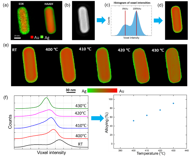
Figure 1.  (a) 2D EDX mapping and forward projection of a 3D HAADF-STEM reconstruction of a Au@Ag nanorod. (b) Slice through 3D HAADF-STEM reconstructions of the nanorod. (c) Histogram of voxel intensities inside the nanoparticle. Estimated intensity values for pure Au and pure Ag are indicated by red vertical bars. (d) Color map of elemental distribution inside the slice of the nanoparticle before heating, where red corresponds to pure Au and green to pure Ag. (e) Slices through quantified 3D HAADF-STEM reconstruction of a Au@Ag nanorod at different temperatures, which are selected according to the alloying behavior. (f) Evolution of the histogram of voxel intensities in the reconstruction of the nanoparticle during alloying (left chart) and the corresponding quantified progress of alloying (right chart).

Uncaptioned visual

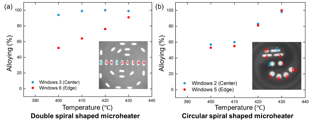
Figure 2. Comparison of the quantified alloying dynamics for Au@Ag nanorods located at different windows on two types of nanochips (a) Double spiral shaped microheater (old design), (b) Circular spiral shaped microheater (new design).


References

[1]    L. F. Allard, et al. A New MEMS-Based, System for ultra-high-resolution imaging at elevated temperatures, Microsc. Res. Tech. 72 (2009) 208–215

[2]    W. Albrecht, et al. Single Particle Deformation and Analysis of Silica-Coated Gold Nanorods before and after Femtosecond Laser Pulse Excitation. Nano Lett. 16 (2016) 1818-1825

[3]  H. H. Pérez-Garza et al. The ʻClimateʼ system: Nano-reactor for in-situ analysis of solid-gas interactions inside the TEM. IEEE 11th Annu. Int. Conf. Nano/Micro Eng. Mol. Syst. (NEMS), (2016) 85-90

[4]  F. Niekiel, et al. Local temperature measurement in TEM by parallel beam electron diffraction. Ultramicroscopy. 176 (2017) 161–169

[5]  J. E. S. van der Hoeven, et al. In Situ Observation of Atomic Redistribution in Alloying Gold-Silver Nanorods. ACS nano. 12 (2018) 8467-8476

[6]  A. Skorikov, et al. Quantitative 3D Characterization of Elemental Diffusion Dynamics in Individual Ag@Au Nanoparticles with Different Shapes, ACS Nano. 13 (2019) 13421-13429

[7]  D.B. Williams, C. B. Carter. Transmission Electron Microscopy. Springer: New York, 2009.

[8] This work was supported by the Marie Skłodowska-Curie Innovative Training Network MUMMERING (Grant Agreement no. 765604). The authors acknowledge financial support from the European Commission through project fundings.


16:00 - 16:05

80 Optimisation of STEM-EDX Characterisation for Fragile Materials: A Case Study of Halide Perovskites

Felix Utama Kosasih, Giorgio Divitini, Caterina Ducati
Department of Materials Science and Metallurgy, University of Cambridge, Cambridge, United Kingdom

Abstract Text

One of the most popular technique in scanning transmission electron microscopy (STEM) is energydispersive X-ray (EDX) spectroscopy. However, due to the limited space in a TEM column, EDX detectors cover a collection solid angle of only 0.1-0.9 sr. This poor collection efficiency becomes an obstacle when dealing with materials which are easily damaged by the electron beam, such as halide perovskites which have come into prominence for its photovoltaic properties.[1] In this work, we systematically examine the trade-off between beam damage and STEM-EDX data quality by varying acquisition conditions on a well-studied halide perovskite solar cell (PSC) architecture. We define and test several metrics to quantify beam damage and data quality, and then demonstrate spatial rebinning as a powerful method to reduce statistical errors. The principles outlined herein can be extended to characterisation of other soft and composite materials with high-energy probes.

The sample is a PSC containing a Cs0.06FA0.79MA0.15Pb(I0.85Br0.15)3 perovskite layer (Fig. 1). A crosssectional lamella was prepared using focused ion beam milling (FEI Helios FIB/SEM), then transferred to a FEI Tecnai Osiris FEG-TEM, minimising air exposure to ~2 minutes. This TEM was equipped with a Bruker Super-X SDD system with a collection solid angle of ~0.9 sr. STEM-EDX spectrum images (SIs) were acquired using a series of electron doses by varying the beam current and dwell time.

These SIs were then denoised with principal component analysis (PCA) in HyperSpy.[2] 

Uncaptioned visual 

Figure 1 Scheme of the solar cell stack used in this study. mp- = mesoporous, c- = compact, FTO = fluorine-doped tin oxide.

We collected STEM-EDX SIs using a spatial sampling of 10 nm/pixel and various beam current (64, 107, 155, 242 pA) and dwell time (10, 30, 50 ms/pixel) values, resulting in 12 electron doses ranging from 400 e-2 to 7560 e-2. To obtain a quantitative measure of beam damage, we monitored changes in X/Pb (X=I,Br) STEM-EDX peak intensity ratios as the dose was increased. We also acquired a high-angle annular dark field (HAADF) image before and after the EDX scans. The after/before ratio of these images’ average intensities is used as another proxy for beam damage. The intensity (I) of a HAADF image is proportional to specimen thickness (t) and its effective atomic number (Zeff) as follows:[3]

                                                                        𝐼 ∝ 𝑡𝑍𝑒𝑓𝑓1.8                                                                                                                                         (1)

Intensity reduction can thus be interpreted as mass loss due to beam damage. The data show that the I/Pb ratio and HAADF intensity ratio decline exponentially with dose, while the Br/Pb ratio stayed approximately constant before dropping only at the highest dose (Fig. 2). This suggests that perovskite damage is dominated by iodine loss, in good agreement with previous studies.[4-6] Using a simple model to relate HAADF intensity decline to iodine loss, we found that both EDX I/Pb ratio and HAADF intensity ratio point to a loss of 0-15% of all iodine atoms in the dose range examined. This highlights the need to minimise electron dose.

Uncaptioned visual 

Figure 2 (a) After/before HAADF intensity ratio and (b) halide/Pb mean peak intensity (MPI) ratio. Both (a) and (b) are plotted semi-logarithmically against electron dose. The dashed trendlines are only to guide the eye and do not represent measured data.


The quality of the PCA-treated EDX data was then examined. First, we check the peak detectability (PD) of the Pb-Lα, I-Lα, and Br-Kα peaks, the elemental lines of highest interest for perovskite. A peak is considered detectable at a 99% confidence interval (CI) if


                                                                                 𝐼 ≥ 3√𝐵                                                                                                                                                     (2)

where I is the background-corrected peak intensity and B is the background intensity.[7] The I-Lα and Pb-Lα peaks are easily detectable even with the lowest dose, but the Br-Kα peak only becomes consistently detectable with a dose of 2910 e-2 (Fig. 3).


Uncaptioned visual 

Figure 3. Maps of STEM-EDX PD at a 99% CI and reference HAADF images acquired before STEM-EDX mapping. Red-shaded pixels are detectable while blue-shaded pixels are not. The red/blue shading indicates how far a pixel’s peak intensity is from the critical value (white) needed to achieve detectability. The maps’ spatial resolution is 10 nm/pixel. Scale bar represents 0.4 μm and applies for all maps and images.


We then evaluate the EDX relative error (RE) at a 95% CI, here taken as the error in the measurement of background-corrected peak intensity I at each pixel, averaged across n pixels identified as a specific compound, in this case perovskite. As X-ray counts follow Gaussian statistics, RE can be calculated as:  

                                                                   𝑅𝐸 Uncaptioned visual                                                                                                         (3)

The RE remains high even at the highest dose, with values of 33%, 24%, and 74% for Pb-Lα, I-Lα, and Br-Kα respectively. A more accurate assessment of composition can be made on a many-pixel basis through spatial rebinning. This step transforms (a portion of) the original SI into a new one with fewer pixels by summing data from a few neighbouring pixels into one pixel. Spatial rebinning thereby reduces RE (for the new SI’s individual pixel) and enables a more accurate quantification at the cost of lower spatial resolution (Fig. 4). It is also a powerful approach to achieve PD without resorting to high doses (Fig. 4).

Uncaptioned visual

Figure 4 Effect of spatial rebinning on (left) RE for EDX SIs acquired with electron doses of 400 and 4840 e-2 and (right) spatial resolution of elemental maps and peak detectability. Scale bar represents 0.4 μm and applies for all maps and images.

Our results show that pixel-by-pixel quantification at 10 nm/pixel spatial resolution suffers from a large error at the dose range examined. Further increase of the electron dose is undesirable due to aggravation of beam damage. However, we can gather data from many pixels in an SI through spatial rebinning to achieve sufficient statistical confidence for quantification of the elements of interest. Depending on the level of precision and resolution desired, one may obtain information from both the original and rebinned SIs. The original SI provides qualitative elemental maps showing compositional heterogeneity at high spatial resolution, while the rebinned SI supplies accurate quantitative compositions for specific areas of interest.

References

[1] H. J. Snaith, Nat. Mater. 2018, 17, 372.

[2] F. de la Peña, V. T. Fauske, P. Burdet, E. Prestat, P. Jokubauskas, M. Nord, T. Ostasevicius, K. E. MacArthur, M. Sarahan, D. N. Johnstone, J. Taillon, A. Eljarrat, V. Migunov, J. Caron, T. Furnival, S. Mazzucco, T. Aarholt, M. Walls, T. Slater, F. Winkler, B. Martineau, G. Donval, R. McLeod, E. R. Hoglund, I. Alxneit, I. Hjorth, T. Henninen, L. F. Zagonel, A. Garmannslund, A. Skorikov, 2018, DOI 10.5281/zenodo.1469364.

[3] P. Hartel, H. Rose, C. Dinges, Ultramicroscopy 1996, 63, 93.

[4] M. U. Rothmann, W. Li, Y. Zhu, A. Liu, Z. Ku, U. Bach, J. Etheridge, Y.-B. Cheng, Adv. Mater. 2018, 30, 1800629.

[5] S. Chen, X. Zhang, J. Zhao, Y. Zhang, G. Kong, Q. Li, N. Li, Y. Yu, N. Xu, J. Zhang, K. Liu, Q. Zhao, J. Cao, J. Feng, X. Li, J. Qi, D. Yu, J. Li, P. Gao, Nat. Commun. 2018, 9, 4807.

[6] S. Chen, Y. Zhang, X. Zhang, J. Zhao, Z. Zhao, X. Su, Z. Hua, J. Zhang, J. Cao, J. Feng, X. Wang, X. Li, J. Qi, J. Li, P. Gao, Adv. Mater. 2020, 2001107, 2001107.

[7] D. B. Williams, C. B. Carter, The Transmission Electron Microscope, 1996.


16:05 - 16:10

434 Influence of experimental conditions on localized surface plasmon resonances measurement by EELS

Dr. Michal Horák1, Tomáš Šikola1,2
1CEITEC Brno University of Technology, Brno, Czech Republic. 2Institute of Physical Engineering, Brno University of Technology, Brno, Czech Republic

Abstract Text

Localized surface plasmon resonances (LSPR) are self-sustained collective oscillations of free electrons in metal nano- and microstructures. Mapping of LSPR with high spatial and energy resolution is necessary to understand their origin and properties. Scanning transmission electron microscopy (STEM) combined with electron energy loss spectroscopy (EELS) has become a standard technique to map LSPR with a nanometer spatial and 10meV to 100meV energy resolution over the last 15 years. It utilizes an electron beam that interacts with the plasmonic antenna and excites the LSPR. EELS measures the energy transferred from electrons to the LSPR and it is sensitive to the electric near field of LSPR.

Despite that many works dealing with EELS measurement of LSPR have been published, there is no experimental work discussing the experimental conditions during the measurement. Such an instructive overview has been missing in literature making it especially difficult for the beginners in the field. Experimental parameters of the STEM-EELS measurement may influence obtained results. Many publications include incomplete information about these parameters or miss them completely. Moreover, even if they are in the literature completely included, one can find several different approaches.

We have experimentally studied the influence of the primary beam energy and the collection semi-angle on the localized surface plasmon resonances measurement by STEM-EELS [1]. We discuss the impact on experimental characteristics which are important to detect localized surface plasmon peaks in EELS successfully, namely: the intensity of plasmonic signal, the signal to background ratio, and the signal to zero-loss peak ratio considering a limited dynamic range of the spectrometer camera.

In the first experiment, we take a series of 3 rods and do the STEM-EELS measurement at the primary beam energy of 300 keV, 120 keV, and 60 keV while keeping the convergence angle at 10 mrad ant the collection semi-angle constant at 20.5 mrad. Figure 1(a) shows EEL spectra of one rod recorded at different beam energies. We clearly see that the signal corresponding to the LSPR is the strongest for the 60 keV electron beam and the weakest for the 300 keV electron beam. This experimental finding is in a perfect agreement with the theory represented by BEM simulation of EEL spectra shown in Figure 1(e). Moreover, if we consider the second peak in experimental EEL spectra in Figure 1(a) at 1.76 eV corresponding to the longitudinal quadrupole mode, we see that lower beam energies are better for observation of weaker plasmon modes.

If we consider measured raw EEL spectra in Figure 1(a), we clearly see that the peak at 1.08 eV corresponding to the longitudinal dipole mode is the most noticeable when using 120 keV electron beam. In the case of 300 keV electron beam the background is enhanced by relativistic effects like the Čerenkov radiation as the speed of the 300 keV electron is higher than the speed of the light in the silicon nitride membrane with the refractive index around 2. On the other hand, the raw EEL spectra measured with a 60 keV electron beam has the highest background in the lower energy loss region. This is caused by a higher probability of scattering events as the inelastic mean free path of electrons in the sample is smaller.

Uncaptioned visual

Figure 1: EEL spectra of the same rod at different beam energies: (a) measured raw EEL spectra and extracted signal; (b-d) STEM annular dark field (ADF) images of the rod with marked area for integration of EEL spectra in (a) recorded during STEM-EELS mapping at 300 keV (b), 120 keV (c), and 60 keV (d); (e) simulated EEL spectra by BEM. Electron beam was situated 5nm outside the rod at the middle of its shorter edge and calculated loss probability density was recalculated to loss probability at 0.01 eV energy intervals (corresponding to the dispersion of the spectrometer in the experiment).

In the second experiment, we take a series of 3 rods and do the STEM-EELS measurement while changing the collection semi-angle from 1.3 mrad to 20.5 mrad at every primary beam energy of while keeping the convergence angle at 10 mrad. We have found that the collection semi-angle is generally not as critical parameter as the primary beam energy. Using the primary beam energy of 300 keV, the collection semi-angle should be preferentially much smaller than the convergence semi-angle, but it is not a critical mistake to use the collection semi-angle larger than the convergence semi-angle. In the case of a medium primary beam energy (represented by 120 keV), the collection semi-angle is not a critical parameter. Using a low primary beam energy (represented by 60 keV), the collection semi-angle should be preferentially the same as the convergence semi-angle.

To conclude, the best results in terms of the best signal to background ratio are obtained using medium primary beam energy, in our case 120 keV, and almost arbitrary collection semi-angle as it is not a critical parameter at this primary beam energy [2].

References

[1] M Horák, T Šikola, arXiv: 2002.04260 (2020).

[2] Supported by MEYS CR under the projects CzechNanoLab (LM2018110, 2020-2022) supporting the CEITEC Nano Research Infrastructure and CEITEC 2020 (LQ1601). M. H. acknowledges the support of Thermo Fisher Scientific and CSMS scholarship 2019.


16:10 - 16:15

147 Investigations into high temperature in-situ SEM imaging of metallic materials.

Miss Rhiannon Heard, Prof Clive Siviour, Dr Kalin Dragnevski
University of Oxford, Oxford, United Kingdom

Abstract Text

Summary

The development of a new heat stage that can be used within a commercial Scanning Electron Microscope (SEM), without the need for shielding or detector modification has facilitated Electron Backscatter Diffraction (EBSD) and Secondary Electron (SE) imaging at temperatures up to 920 °C. This study demonstrates the effects of magnetism, surface finish and oxidation on the ability to track microstructural changes at these temperatures in-situ. The applications focus is on capturing grain growth and phase transformations of Fe and Ni based alloys using novel thermal etching-based imaging approach, supplemented by EBSD. These unique observations document unusual grain growth patterns and provide in-sight into the microstructural and crystallographic changes that occur during phase transitions. 


Introduction

In-situ high temperature SEM imaging enables observation and subsequently improves understanding of the behaviour of the materials' microstructure by recording changes in grain size and phase during heating. Some success is documented of imaging using a variety of one-off experimental set-ups, such as capturing Electron Back Scatter Diffraction (EBSD) images at temperatures between 700 °C and 1450 °C with the use of shielding [1] and/or detector modifications [2]. However, shielding greatly reduces the imaging area and detector modifications would not be suitable for use in a wide variety of microscopes. This study demonstrates the advantages, challenges and applications of a novel heat stage developed for experimental in-situ high temperature SEM imaging without the need for shielding or detector modification. In particular, the data provides understanding about the specific microstructural evolution during the heat treatment processes of Ni and Fe-based alloys.


Method

The heat stage, consisting of a button heater, combined with a purpose built mounting, cooling and temperature control system, initially underwent testing using industrially pure nickel specimens, which were heated to 850 °C and imaged using SE and EBSD within a Zeiss EVO SEM. Subsequent experiments were conducted on 0.4% carbon steel imaged at temperatures of up to 920 °C. From the SE images it was possible to track the grain growth owing to a phenomenon known as thermal etching [3]. To support the in-situ microstructure data gathered, chemically etched samples were also imaged optically before and after heating and change in microstructure quantified.


Results & Discussion

The Nickel EBSD maps and images (Fig. 1) at temperature demonstrate the success of the stage and the benefit of in-situ thermal etching. However, the nickel EBSD data was affected by the magnetic phase change at the Curie Temperature; where a loss of EBSD image quality was observed, which was regained when temperatures increased. The in-situ high temperature thermal etching technique was also used to study the grain growth mechanisms of carbon steel in the austenitic region. The results indicated that abnormal linear grain growth occurred during the in-situ experiments, which may be due to some remaining ferrite grains shrinking as austenite grows. This is supported by the EBSD phase change data. 

To further investigate this, ex-situ grain growth studies on thermally etched specimens was carried out at different temperatures. The grain growth ex-situ at the surface and bulk post a 4-hour heat treatment at 800, 850 and 920 ºC indicates a negative correlation between temperature and surface grain growth, but a positive correlation between temperature and bulk grain growth.  This is due to the oxidation rate increasing with temperature, which leads to pinning of the grain boundaries around the thermal etch on the surface, thus stalling grain growth and indicating that the surface may not 

always represent the bulk. However, oxidation is minimal when heating for 1 hour at 800 ºC and thus in-situ surface grain growth can be deemed representative of the bulk of the material. 

Conclusion 

In-situ high temperature imaging is highly beneficial in quantifying changes in phase and microstructure, but is affected by magnetism, surface finish and oxidation. It also provides insight into the effect of heat treatments on the bulk verses surface of a material and how sample preparation and atmosphere can impact this. If oxidation on the surface is limited or inhibited, then thermal etching can be adopted as an alternative and novel method to monitor changes in microstructure in-situ at elevated temperatures


Uncaptioned visual

Figure 1. Graphical Abstract visualising the newly developed heat stage and the main findings of this study. (a) Image of heat stage. (b) EBSD of Steel phase change showing before heating at room temperature and during change at 800 °C. (c) SEM images at 800 °C of thermally etched Steel with grain boundaries outlined. (d) Raw (uncleaned) EBSD images of Nickel at temperature intervals during heating up to 800 °C. (e) Ex-situ grain growth data showing the grain size pre-heating and in the bulk and surface after 4 hours in-situ heating. 


References

References

[1] I. Lischewski et al, Texture, Stress and Microstructure (2008), p.1.

[2] G. Gregori et al, Journal of Electron Microscopy Microscopy (2002),p.347. 

[3]  W. Mullins, Journal of Applied Physics 28 (1957), p.333.


16:15 - 16:20

734 EDX quantification in the TEM: How to measure ζ-factors without knowing the sample thickness

Nikolaus Rauch, Judith Lammer, Sebastian Rauch, Martina Dienstleder, Werner Grogger
Institute of Electron Microscopy and Nanoanalysis (FELMI), Graz University of Technology & Graz Centre for Electron Microscopy (ZFE), Graz, Austria

Abstract Text

Within this abstract, we present a new way to determine 𝜁-factors for EDXS quantification experimentally for both light and heavy elements. With this approach, we eliminate the necessity of knowing the thickness of the reference sample, which is very often a crucial issue during 𝜁-factor determination.

The correct determination of the element concentration in a material via energy-dispersive X-ray spectrometry (EDXS) stands or falls on the precision of the quantification method. There are two established methods within the TEM community: the conventional Cliff-Lorimer technique [1] and the newer 𝜁-factor method [2]. The latter provides not only elemental concentrations but also the mass-thickness of the observed specimen area as results. Furthermore, a proper absorption correction for low energy X-rays is implemented, which makes it more accurate for the quantification of light elements. A precondition for using this method is the determination of correct sensitivity factors, the so-called 𝜁-factors. However, the determination of accurate values for light elements is a complex and challenging task, which is the reason, why the method is unfortunately not as commonly used as suspected regarding its major advantage of a built-in absorption correction.

One major drawback during the experimental acquisition of 𝜁-factors is the fact that the thickness of the reference sample must be known. This either limits the researcher to reference materials with known thickness or brings in an additional uncertainty in thickness measurement.

To overcome the problem of absorption effects during 𝜁-factor acquisition Marvel et al. [3] recently applied an imaginative ansatz: They used binary systems – where the heavier element possesses a non-absorbing (high-energy) X-ray line and its 𝜁-factor is known, while the X-ray line of the light element is strongly affected by absorption – and measured intensities of both X-ray lines on several thicknesses of the sample. Afterwards they plotted the k-factor over the non-absorbing X-ray line to obtain a graph called ‘Horita-plot’ [4]. Extrapolating the exponential fit to zero thickness yields the absorption-free k-factor and – if one 𝜁-factor is already known – the 𝜁-factor for the other element.

We took up this idea and expanded the approach of using exponential fits in Horita-plots in order to determine both 𝜁-factors without knowing the actual thickness of the sample. We did this through rearranging the physical expression for the intensity of an X-ray peak and linking it to the fitting parameters of the exponential fits in Horita-plots (fig. 1).

We used three samples (SiO2, SiC and ZnO) with different absorption properties. We measured X-ray spectra at several thicknesses and plotted the intensities using Horita-plots (fig. 2a). Thereafter, we performed an exponential fit and calculated the 𝜁-factors from the fitting parameters. The accuracy of the fitting parameters - and subsequently of the 𝜁-factors - benefits from large absorption values. We determined adequate limits for mass absorption coefficients and take-off angles in order to a priori choose reasonable samples and experimental conditions.

In addition, we modified the Horita-plots and used t/λ-values obtained from electron energy loss spectroscopy as independent parameters for the thickness on the abscissa (fig. 2b). Using these relative thickness values further improved the accuracy of the obtained 𝜁-factors. When doing so, one does not only retrieve the 𝜁-factors for both X-ray lines, but also the inelastic mean free path of the sample.

With this work we contribute to the aim of EDXS becoming more feasible and accurate for the quantification of light elements: we used the absorption effect of low X-ray lines to our advantage and brought up a simple way to determine ζ-factors of both light and heavy elements at a time without knowing the sample thickness [5].

Uncaptioned visual

Figure 1: The ratio of two X-ray intensities IA and IB from the elements A and B – where IA is partially absorbed within the specimen, while IB does not suffer from absorption – describes the exponential behaviour within a Horita-plot. This relation depends on both ζ-factors and several parameters, which are summarized as two constants in the equation. If all parameters are known, the ζ-factors for both elements can be obtained from the fitting parameters of the exponential fit as given in fig. 2a.


Uncaptioned visual

Figure 2: a) Horita-plot: intensity-ratio over non-absorbed intensity (sample ZnO). ζ-factors are obtained from the fitting parameters of the exponential fit. b) Modified Horita-plot: intensity of the absorbed X-ray line over the t/λ values (sample ZnO).


References

[1] G Cliff and GW Lorimer, Journal of Microscopy 103 (1975), p. 203–207

[2] M Watanabe and DB Williams, Journal of Microscopy 221 (2006), p. 89–109

[3] CJ Marvel et al, Ultramicroscopy 202 (2019), p. 163–172

[4] Z Horita et al, Journal of Microscopy 143 (1986), p. 215–231

[5] The support of the European Union Horizon 2020 programme (grant 823717–ESTEEM3) is gratefully acknowledged.


16:20 - 16:25

887 HOLZ-STEM imaging of Ordering in Double Perovskite Thin Films

Mr Thomas Macgregor, Dr Ian MacLaren
University of Glasgow, Glasgow, United Kingdom

Abstract Text

Summary

The recording and analysis of scanned diffraction and 4D-STEM data using the latest generation of fast pixelated detectors has enabled significant advances in both quality and acquisition speed.  Herein the use of hybrid pixelated detectors, along with custom Python-based coding libraries,  is demonstrated. Python – based coding tools are used to browse the collected data, isolate diffraction features of interest and store the data in a compressed format in order to fit memory of a typical personal computer 1–4.  This is used to find the intensity in HOLZ rings as a function of the probe position in datasets recorded from thin films of double perovskites grown on perovskite substrates.

As previously shown, the Higher Order Laue Zone (HOLZ) ring intensity is a good proxy for the degree of atomic modulation along a column of atoms (especially heavy A-site atoms), and this is used to determine how the modulation varies with distance from the interface.  This information is critical to the growers as it correlates to the development of the required size modulation in B-site spaces, which is in turn a key driver of the double perovskite ordering process.  It is demonstrated that this technique can be used along both <100> and <110> directions in the primitive perovskite cubic cell, and in both cases yields useful information about atomic modulation.  

Introduction

The combination of direct electron detectors with a Scanning Transmission Electron Microscope (STEM) instrument allows for the collection of four-dimensional datasets (4D-STEM) where a diffraction pattern (DP) is collected for pixel in the selected scanning area. By applying a virtual annular aperture to  the processes 4D-STEM data the conditions for HAADF, MAADF and LAADF can be replicated from a single dataset.

While HAADF imaging provides atomic number, (Z)-contrast, information from a specimen, each image only provides a 2D perspective on the specimen. With the aid of a direct electron detector, it is also possible to observe HOLZ rings during a scan, and then analyse their position and intensity in post-processing.  This allows for the imaging of the 3D- ordering within the specimen as the periodic positional modulation of atoms along a specific atomic columns can lead to the appearance of additional HOLZ rings due to the formation of a longer period superstructure to the unit cell along the beam direction  5,6 .

By adjusting microscope conditions to produce a highly convergent probe and selecting a suitable camera length it was possible to collect suitable 4D-STEM datasets with DPs covering the full angular range transmitted by the microscope and allowing the observation of the HOLZ rings.  This technique, termed HOLZ-STEM, has then been used to observe the 3D structure of the different materials at atomic resolution.

Methods

Samples of thin epitaxial perovskite oxides on standard samples were prepared elsewhere, in the group of Prof Judith L. Driscoll (University of Cambridge).  These were prepared for electron microscopy by a standard FIB liftout method.  Scanning transmission electron microscopy was performed using an aberration corrected JEOL ARM200cF operated at 200 kV and a convergence semiangle of 29mrad, with datasets recorded at both atomic  and at slightly lower resolutions.  Data was collected using a 4D-STEM approach using a Merlin for EM detector (Quantum Detectors Ltd.) with the microscope camera length set to either 20 or 40 cm, and the acquisition using a custom designed MERLIN PixSTEM plugin developed by Nord et al. 7.

Results and Discussion

Figure 1 shows the processing of the datasets to a useful signal using the example of La2CoMnO6 (LCMO) grown on LSAT ((LaAlO3)0.3(Sr2TaAlO6)0.7) 8.  Each pixel of the dataset contains a high angle DP containing Kikuchi lines and Higher Order Laue Zones (HOLZ) rings, Figure 1a shows an example from one representative pixel in the LCMO thin film. A second perovskite system consisting of a La2MnNiO6 (LMNO) thin film grown on an SrTiO3 (STO) was also measured.

 After running centre finding on each diffraction pattern, these are converted to a 1D profile of intensity versus radius (either in pixels or calibrated into units of angle), as shown in Figure 1a.  Figures 1b and 1c show the results of subtraction the fitted background, the signals were cropped to show the distribution between 20 and 160 mrad scattering angle after calibration. The calibration process was carried by using the expected FOLZ radius for the SrTiO3 along [110] of 95.38 mrad. After calibration the double perovskite signal was observed at 64.58 mrad with is very close to the predicted value (67.43 mrad).

In Figure 1d shows an image created from the intensity in. the inner HOLZ ring, the majority of the remaining signal intensity is located  on A-site atoms in the LCMO film, which makes sense as this should have some period doubling and atomic modulation along this direction with the formation of the double perovskite structure.  The LSAT is dark as it does not have the same atomic modulation or cell doubling.  

Whilst this has been performed along the [110] direction in one double perovskite, similar results have been achieved for another double perovskite (La2MnNiO3) along [100], although the signals are weaker.  Results from both [100] and [110] projections will be discussed in the conference presentation.  Specifically, this will then be used to determine the strength of atomic site modulations along A-site columns as a function of distance from the interface and to correlate that with B-site ordering as determined by other techniques (such as EELS mapping).

Uncaptioned visual 

Figure 1: Demonstration of the HOLZ STEM processing on a LCMO-LSAT specimen along the [110] direction of the primitive perovskite cell: a) fitting a power-law background to the high angle scattering to isolate the signal after radial integration b) the subtracted FOLZ signal for SrTiO3 after angle calibration was applied c)  the subtracted signal from an area in LCMO film showing a strong inner Laue zone arising from period doubling in the double perovskite d) the HOLZ-STEM image created from the intensity in this inner Laue zone, the brighter regions highlight just the LSAT-LMCO layers.

References

[1]       “FPD: Fast pixelated detector data storage, analysis and visualisation. https://gitlab.com/fpdpy/fpd (accessed May 1, 2019),” https://gitlab.com/fpdpy/fpd. 2019.

[2]       G. Paterson, R. Webster, M. Nord, K. Paton, and A. Doye, “FPD: Fast pixelated detector data storage, analysis and visualisation.” 2019.

[3]       R. Ballabriga, M. Campbell, E. Heijne, X. Llopart, L. Tlustos, and W. Wong, “Medipix3: A 64k pixel detector readout chip working in single photon counting mode with improved spectrometric performance,” Nuclear Instruments and Methods in Physics Research Section A: Accelerators, Spectrometers, Detectors and Associated Equipment, vol. 633, no. SUPPL. 1, pp. S15–S18, May 2011.

[4]       R. Plackett, I. Horswell, E. N. Gimenez, J. Marchal, D. Omar, and N. Tartoni, “Merlin: a fast versatile readout system for Medipix3,” Journal of Instrumentation, vol. 8, no. 01, pp. C01038–C01038, Jan. 2013.

[5]       F.-T. Huang et al., “Scanning Transmission Electron Microscopy Using Selective High-Order Laue Zones: Three-Dimensional Atomic Ordering in Sodium Cobaltate,” Physical Review Letters, vol. 105, no. 12, p. 125502, Sep. 2010.

[6]       V. Randle, I. Barker, and B. Ralph, “Measurement of Lattice Parameter and Strain Using-Convergent Beam Electron Diffraction,” 1989.

[7]       M. Nord et al., “Fast Pixelated Detectors in Scanning Transmission Electron Microscopy. Part I: Data Acquisition, Live Processing and Storage,” 2019.

[8]       The authors gratefully acknowledge funding from the EPSRC under grant number EP/P013945/1.


16:25 - 16:30

1038 Organic Adhesion Layers – A Smart Way to achieve an Ultrathin Au Film for Plasmonic Applications

Mario Heinig1, Alice Bastos da Silva Fanta1, Dipanwita Chatterjee2, Antonius van Helvoort2, Håkon Ånes2, Mériem Er-Rafik1, Jakob Birkedal Wagner1, Shima Kadkhodazadeh1
1Technical University of Denmark, Lyngby, Denmark. 2Norwegian University of Science and Technology, Trondheim, Norway

Abstract Text

The fabrication of ultrathin gold films for plasmonic and microelectronic devices require an adhesion layer to guarantee reliable bonding to the dielectric substrate and maintain the noble metal thin film properties. Organic linkers, as 3-aminopropyl­-trimethoxysilane (APTMS) and 3-mercaptopropyl-trimethoxysilane (MPTMS) are used to adhere gold to silicon dioxide substrate [1,2]. These organosilanes build a self-assemble monolayer on the SiO2 substrate and enable the fabrication of continuous Au films with a thickness down to 6nm and surface roughness below 0.5nm [3]. The influence of these adhesion layers on the Au film microstructure, especially linked to the performance, is not well understood and a comparison study across different length scales and the effect of the adhesion promoters is necessary. Another aspect is the thermal stability and response of the organic adhesion layers, which are of consequence for many applications, including photovoltaics [4] and optical sensors [5].
Here, we have studied the effect of the organic adhesion layers APTMS and MPTMS on the microstructure, chemistry and electrical/optical properties of ultrathin Au films. The microstructure of the Au films are investigated in the same area using transmission Kikuchi diffraction (TKD) in a SEM and scanning precession electron diffraction (SPED) in TEM. The adhesion layers affect the microstructure (i.e. grain size and texture) of the fabricated polycrystalline Au films. Figure 1 illustrates orientation maps of 10nm thick gold films on APTMS, MPTMS and reveal differences in the degree of texture. Furthermore, we carry out an in-situ thermal study in order to reveal changes in microstructure in response to heating, and to determine the operation range of the organic adhesion layers. These results contribute to the systematic optimisation of the fabrication process of ultrathin Au films for advanced plasmonic and microelectronic devices.

Uncaptioned visual

Figure 1 Orientation maps of a gold thin film (10nm thickness) with MPTMS (left) and APTMS (right) as adhesion layer on a SiO2 substrate. The microcrystalline structure of the Au grains are shown by TKD scans, while the selected area illustrates a SPED measurement of the same region with scale bars of 50nm.

References

[1] Sukham et. al., ACS Appl. Mater. Interfaces, 9(2017), p.25049-25056.

[2] Gothe et. al., J. Phys. Commun. 2 (2018) 035005.

[3] Leandro et. al., ACS Applied Materials & Interfaces, 7(2015), p. 5797-5802. 

[4] Ameri et. al., Energy Environ. Sci., 2(2009), p.347-363.

[5] Ali et. al., Material Science and Engineering C 28(2008), p.628-632.


16:30 - 16:35

94 In-situ liquid TEM study at early stage of sweet corrosion

Ms Surabhi Agrawal1, Dr Mobbassar Hassan Sk1, Dr Richard Langford1, Prof. Stuart Clarke2
1University of Cambridge, Cambridge, United Kingdom. 2University of Cambridg, Cambridge, United Kingdom

Abstract Text

Iron and steel corrode in carbon dioxide saturated low oxygen brine environment forming iron carbonate products; commonly known as sweet scales.Economic and environmental consequences of sweet corrosion in oil-field components are severe. Deeper understanding of this process is of great scientific and commercial interest, as it underpins new and efficient solutions to corrosion control, e.g. templated scale formation to more protective scales and facilitate more reliable corrosion prediction models and better estimates of the time interval between maintenance checks and component replacement. Here we address this issue by studying the process of sweet scaling at the very early stage - at a spatial resolution which can resolve scale nucleation event. 

Uncaptioned visual

Figure 1: Siderite crystals of FeCO3

Despite the importance of early stages of the phenomena, the earlier works has been largely limited to speculation based on ex-situ studies of iron and steel pieces exposed to solution of commercial interest.2 Moreover, ex-situ characterisations with all likelihood entail the transformation of the corrosion product upon removal of samples from the solution, and once they are exposed to air. Therefore, it is crucial to observe and understand the process from its very early stage in-situ. Moreover, although it is appreciated for a fact that the local environment2-5, which is different from the global environment, plays a critical role in nucleation and evolution of the scale, it is not clear how the local conditions determine the kinetics of the process, mineralogy, morphology and eventually stability of the scale. 

We used Transmission Electron Microscopy (TEM) to study formation of iron carbonate on thin iron films (~30nm thickness) in low oxygen and carbon dioxide saturated salt solution at pH 7.5. Hummingbird scientific liquid flow TEM holder was employed for this in-situ study. We addressed the key questions with regards to the heterogeneity of nucleation process, nature (amorphous/crystallinity) of the corrosion product and its evolution. Bright/Dark field imaging combined with diffraction pattern study is employed to study the nature of the reaction product. 

Uncaptioned visual 

Uncaptioned visual

Figure 2. (a) Bright field in liquid in-situ TEM imaging shows the growth of product along the grain boundaries of the iron film. (b) Selected area diffraction at these product sites indicates that the material formed were crystalline.

Nuclei appear to grow along the grain-boundaries of the iron film (figure 2(a)). Random growth of species on the iron film surface suggests that the nucleation is heterogeneous. Another key feature is that the species, presumed to nucleus, give a strong diffraction pattern with spots unique to the iron film, revealing that nuclei observed is crystalline (figure 2(b)). On the basis of our preliminary finding, we present a hypothetical mechanism for nucleation under the observed chemical conditions (figure 3), which is currently under process of reconfirmation.  

Uncaptioned visual

Figure 3: Reaction mechanism for the formation of iron carbonate scale on iron surface.


References

[1] Joshi, G, Elucidating Sweet Corrosion Scales, Ph.D (2016), The University of Manchester.

[2]  M Hassan Sk et al, Corrosion Science 126 (2017), 26.

[3] M Hassan Sk and A.M. Abdullah, International Journal of Electrochemical Science 12 (2017), 4277.

[4] M Hassan Sk et al, Journal of The Electrochemical Society 165 (2018), C278.

[5] S. Lee and H. Xu, Chemical Geology 488 (2018), 180.


16:35 - 16:40

220 From atoms to particles: Hetero- and homogeneous nucleation of sub-nm Pt clusters observed at the atomic scale in liquid

Trond Rypdal Henninen, Debora Keller, Rolf Erni
Empa, Swiss Federal Laboratories for Material Science and Technology, Dübendorf, Switzerland

Abstract Text

The formation of solid matter as modelled by the classical nucleation theory (CNT), assumes to be triggered by the generation of spherical nuclei. However, initially at sub-nm scale, non-spherical atomic clusters form with structures deviating from bulk crystal. Understanding the atom-by-atom growth dynamics at this size, requires considering the individual atoms. Conventional liquid cell holders have enabled studying liquid systems in transmission electron microscopes, but are limited in spatial resolution by the thickness of the liquid and the encapsulating windows (in total 100-1000 nm), making imaging at sub-nm resolution challenging. To further progress to atomic resolution, we use low vapour-pressure liquids, (glycerol or ionic liquids, such as 1-butyl-3-methyl imidazolium chloride).[1] The negligible vapour pressure makes such liquids directly vacuum compatible without windows, and enables atomic resolution in suspended nanofilms and supported nanodroplets (5-50 nm thickness). Furthermore, a melting point above room temperature enables adjusting the viscosity of the liquid, and thus reaction kinetics, by heating. In our liquid phase experiments, we can observe dispersed Pt atoms to nucleate into few-atom clusters, which further coalesce and grow into nanoparticles or disordered cluster agglomerates, or redissolve into the liquid. CNT tells us that the presence of a surface lowers the energy barrier of heterogeneous nucleation, compared to homogeneous nucleation in a liquid phase. In our liquid experiments, there is indeed a corresponding effect, where nucleation is rarely observed in the suspended liquid nanofilms, while easily observable at a high nucleation rate in the nanodroplets on a carbon surface. As the highly unstable sub-nm clusters nucleate and dissolve, increased stability is observed in clusters of ca 8-13 atoms, compared to smaller clusters. Indeed, nucleating clusters typically form directly into this size range, where various close-packed structures (such as fcc and icosahedral[2]) can often be observed. This indicates that the formation of close-packed, crystalline structures, already at the few-atomic scale, is an essential step of the nucleation process.

Uncaptioned visual

Figure 1: Nucleation of a 12-13 atom Pt cluster.  a Initially, there are only individual atoms and small clusters of 2-4 atoms forming. b After 3s, ca 10-11 atoms have come into contact to start forming a cluster. c At 6s, 11-12 atoms. d At 23s, 10-11 atoms. e At 27s, 11-12 atoms. f At 56s, 12-13 atoms. The clusters in d-f show different close-packed structures.


References

References:

[1]       D. Keller, T. R. Henninen, R. Erni, Micron 2019, 117, 16.

[2]       T. R. Henninen, M. Bon, F. Wang, D. Passerone, R. Erni, Angew. Chemie Int. Ed. 2019, 2.

[3]       This project has received funding from the European Research Council (ERC) under the EU's Horizon 2020 research and innovation program (grant No. 681312) 


16:40 - 16:45

240 Fabrication of ferroelectric thin film specimen for in-situ electrical biasing TEM studies by FIB.

Alexander Vogel1,2, Martin Sarott2, Prof. Dr. Manfred Fiebig2, Dr. Morgan Trassin2, Dr. Marta Rossell1
1Swiss Federal Laboratories for Materials Science and Technology, Empa, Dübendorf, Switzerland. 2ETH Zürich, Zürich, Switzerland

Abstract Text

Ferroelectrics have a large variety of applications in modern life. These include piezoelectric actuators, sensors, dielectric capacitors or memory devices. In data storage applications, ferroelectricity presents a unique alternative to ferromagnetism as it allows for more energy efficient and faster devices. However, the commercialization of ferroelectric memory devices has been hindered by major reliability issues [1,2] such as retention loss [3], imprint [4], and fatigue [5]. To overcome these issues, a deeper understanding of the microscopic mechanisms of domain wall motion, nucleation, and the role of various types of defects, such as oxygen vacancies, in this context is required. Even so, at present, there is a lack of dynamical data on the ferroelectric switching process at the atomic scale, which impedes further development in this field.

In this work, we report on the fabrication of ferroelectric thin film specimens for in-situ electrical biasing experiments inside the transmission electron microscope (TEM) by focused ion beam (FIB) to fill this gap in knowledge. The specimens were fabricated on commercial micro-electro-mechanical system (MEMS)-chips manufactured by Protochips that allow for electrical and thermal stimuli without applying external strain on the thin films. A FEI Helios 660 SEM/FIB equipped with an EasyLift Nanomanipulator, operating a Ga ion source with acceleration voltages up to 30 kV, was used to machine the electron transparent specimens. A plate capacitor geometry was adopted to mimic the environment of industrial applications for ferroelectric capacitors. The bottom electrode of the capacitor consists of a conductive substrate, such as Nb-doped SrTiO3, while sputtered Pt and Pt deposited by ion-beam-induced chemical vapor deposition were used as top electrode. The investigated ferroelectric thin films include Pb(Zr0.2Ti0.8)O3 (PZT) and BiFeO(BFO) grown by pulsed laser deposition. 

The specimen geometry was optimized to prevent the mechanical failure of the electrodes caused by the strain induced by the piezoelectric response of the ferroelectric. This allowed for stable PZT thin film specimens, with a film thickness of 100 nm, up to a biasing voltage of 20 V. The investigation of the currents passing through the capacitor in response to the applied voltage revealed a Schottky-diode like behaviour. Typical currents in the reverse-bias direction were on the order of 100 nA at a biasing voltage of 5 V. A thermal breakdown of the lamella occurred once the leakage currents exceed 1 µA, with both the Pt electrode and ferroelectric thin films melting at this point. The initial characterization of the ferroelectric thin films by conventional dark-field (DF) TEM imaging and high-resolution high-angle annular dark-field (HAADF) scanning TEM (STEM) was performed using a FEI Titan Themis microscope equipped with a probe CEOS DCOR spherical aberration corrector operated at 300 kV. In DF-TEM, the correct choice of diffraction spots used for image formation allows for tracking the in-plane or out-of-plane domain distribution in the ferroelectric film. In HAADF-STEM imaging, the ferroelectric polarization is mapped on the atomic scale by a combination of time series averaging [6], probe deconvolution and atomic column fitting [7]. 

Our results provide the path to prepare highly stable ferroelectric thin film capacitor specimens for in-situ S/TEM observations. This shall enable future studies on the dynamic processes in ferroelectric thin films under an applied bias voltage, which are crucial for the practical implementation of these materials in data storage devices [8].


References

[1] O. Auciello, J. F. Scott, and R. Ramesh, Physics Today 51 (1998), p. 22-27.

[2] W. L. Warren, D. Dimos, and R. M. Waser, MRS Bulletin 21 (1996), p. 40-45.

[3] A. Gruverman and M. Tanaka, Journal of Applied Physics 89 (2001), p. 1836.

[4] A. K. Tagantsev et al., Journal of Applied Physics 96 (2004), p. 6616-6623.

[5] A. K. Tagantsev et al., Journal of Applied Physics 90 (2001), p. 1387-1402.

[6] L. Jones et al., Advanced Structural and Chemical Imaging 1 (2015), p. 8.

[7] M. Nord et al., Advanced Structural and Chemical Imaging 3 (2017), p. 9.

[8] The authors gratefully acknowledge funding from the Swiss National Science Foundation under project number 175926.


16:45 - 16:50

640 Hydrodynamic Characterization of Liquid-Phase TEM Sample Holders - towards quantitative in situ Studies of Nanoscale Dynamics

Stefan Merkens1, Joscha Kruse2, Christopher Tollan1, Evgenii Modin1, Marek Grzelczak2,3, Andrey Chuvilin1,3
1CIC nanoGUNE BRTA, Donostia - San Sebastian, Spain. 2Donositia International Physics Center (DIPC), Donostia - San Sebastian, Spain. 3Ikerbasque, Basque Foundation for Science, Bilbao, Spain

Abstract Text

An experimental methodology for quantitative characterization of intermixing in (nano-)fluidic Liquid-Phase Transmission Electron Microscopy systems is presented and verified by numeric model simulations (Figure 1). The gained knowledge is also applied to control nanoscale dynamics in situ by hydrodynamics adjustment of the composition of the reaction solution.

Uncaptioned visual

      Figure 1: Simplified illustration of the experimental method for hydrodynamic characterization of fluidic LP-TEM sample holder. Changes in the contrast of the images obtained in the imaged area upon changes in the applied flow are used to quantify hydrodynamic properties. Finite-element convection diffusion model simulation were conducted to understand fluid mixing dynamics.


Already today Liquid-Phase Transmission Electron Microscopy (LP-TEM) is providing many intriguing opportunities in research areas, ranging from material science to medicine and biology. For instance, the methodology for “just in vivo” imaging of biological and synthetic (nano-) objects, as well as studies of radiation-induced processes (such as crystal nucleation and growth), are being intensively developed.1 However, beyond that there is still one ultimate goal to be realized in the context of chemistry, which is to experimentally mix reagents, to describe a mechanism of chemical reaction between them and to quantify its kinetics by time-resolved in situ visual inspection at the nanoscale.

On the way to this goal, there is a row of challenges to face. The most complex - accounting for and avoiding radiolysis - is being addressed by several fundamental works published by various groups.2,3 Another less fundamental yet crucial challenge is understanding and describing the kinetics of reagents mixing inside the very complex and very confined space of an in-situ chemical reactor.4 In the present work, we describe our theoretical and experimental approaches to this problem and the key results.


To evaluate the mixing experimentally we use an in-situ liquid flow cell system with 2 inlets. This gives external control over the mixing of pure water in one inlet with a solution of an electronically dense reagent solution (acting as a contrast agent to the transmitted beam) in the other inlet. The transmitted intensity across the imaged area are monitored in TEM mode over the entire time span of the flow experiment (about 1 h). In several distinct experiments, the effect of various experimental parameters on the mixing dynamics are probed by a pulse-relaxation method5: the flow characteristics of the supply channels are been periodically switched, and relaxation dynamics have been  measured. This allows: 1) to quantify cell expansion (bumping) upon increase of the hydrodynamic pressure, 2) to study delay times as well as temporal concentration gradients upon switching between different flow conditions both depending on applied total flow rate and fluid channel geometry and 3) to control/calibrate concentration by the applied flow rates ratio. 

Finite element-based computation fluid dynamic (CFD) simulation of diffusion (Fick’s law) and convection (Navier-Stokes equation) are performed for the double inlet in-situ liquid holders series of Protochips, Inc. (Poseidon and Poseidon select®) accounting for the exact shape of internal volume.6 Challenges in the implementation of the model arising from the multiscale flow channel geometry (the premixing channels are on the mm scale, whereas the intermembrane space is of the order of 100 nm) have been overcome by smart definition of the finite element mesh. Thus, the implemented software model can support experimental work by simulating hydrodynamic mixing experiments as well as validating new sample holder geometries. Initial results regarding several experimental parameters, such as applied flow rate and flow rate ratio as well as the internal geometry of the fluidic holder, are studied and show good agreement with experimental results. 

Altogether, our results provide a comprehensive twofold approach for characterizing the complex fluidic environment of LP-TEM sample holder. It further contributes to the development of next generation LP-TEM sample holder systems and allows to systematically design in situ flow experiments to quantify the kinetics of externally triggered nanoscale dynamics. Here, we demonstrate the general feasibility of such studies by showing recently obtained results on both salt-induced self-assembly of nanoparticles in confined space as well as concentration-dependent etching and growth of nanoparticles. We hope that our findings will support the LP-TEM community in better planning their fluidic LP-TEM experiments so that chemical kinetics of externally triggered nanoscale dynamics can soon be quantified by LP-TEM.


References

1.        Jonge, N. de et al. Liquid Cell Electron Microscopy. Liquid Cell Electron Microscopy 1, (Cambridge University Press, 2016).

2.        Schneider, N. M. Electron Beam Effects in Liquid Cell TEM and STEM. Liq. Cell Electron Microsc. 140–163 (2017).  

3.        Schneider, N. M. et al. Electron-Water interactions and implications for liquid cell electron microscopy. J. Phys. Chem. C 118, 22373–22382 (2014).

4.        Ring, E. A. & De Jonge, N. Microfluidic system for transmission electron microscopy. Microsc. Microanal. 16, 622–629 (2010).

5.        Merkens, S. et al. Time-Resolved Analysis of the Structural Dynamics of Assembling Gold Nanoparticles. ACS Nano 13, 6596–6604 (2019).

6.       CAD model of the internal sample holder geometry received from Protochips, Inc. 

7.       Special thanks are extended to the staff of Protochips, Inc. company for the close        collaboration on both experimental and theoretic part of this project.


16:50 - 16:55

1027 Rapid In-situ XANES Imaging of Chemical Gradients during Catalytic Partial Oxidation of Methane

Ms Saba Alizadehfanaloo1, Dr Andreas Schropp1, Mr Martin Seyrich1, Dr Jan Garrevoet1, Scientist Vadim Murzin1, Mr Johannes Becher2, Dr Dmitry Doronkin2, Dr Thomas L. Sheppard2, Prof Jan-Dierk Grunwaldt2, Prof Christian G. Schroer1,3
1DESY, Hamburg, Germany. 2KIT, Karlsruhe, Germany. 3University of Hamburg, Hamburg, Germany

Abstract Text

Supported Rh- and Pt-alumina catalysts are gaining attention for their application in the catalytic partial oxidation (CPO) of methane to synthesis gas (CO + H2), which is a potential alternative to large-scale and energy-intensive steam reforming plants. These catalysts display gradients in oxidation state and temperature along the catalyst bed, during the switch between methane combustion and ignition/extinction of the CPO reaction [1,2]. To obtain meaningful data for this catalytic reaction, it is important to study it in a spatially-resolved manner (in at least two dimensions), and with time and energy resolution under reaction conditions. However, combining all these concepts is a significant challenge. During previous chemical imaging experiments [1-3], the CPO reaction was studied under static operando conditions with data acquisition in the order of a few hours [1,2] or was limited to a single energy point [3], not allowing for spectroscopic imaging. Now by technical advances in imaging (fast high-resolution detectors) and beamlines at PETRA III, it is possible to study chemical reactions under different (non-static) conditions by spatiotemporal chemical imaging, in order to probe the oxidation state and coordination environment of catalysts in a spatially-resolved way. 

Here we demonstrate new opportunities for rapid spatiotemporal chemical imaging, with CPO of methane over a Pt-alumina catalyst as a model study. The method is also readily applicable for multidimensional (spatially, time, energy resolved) imaging of the changes occurring in other complex catalytic materials under operating conditions. We report on X-ray absorption imaging experiments carried out at the advanced spectroscopy beamline P64 at PETRA III. The beamline is equipped with a fast scanning QEXAFS monochromator, which was synchronized with a high-resolution X-ray detector running continuously at 50 Hz full-frame rate. By measuring a rapid sequence of 2D transmission images of the reactor bed around the Pt L3 absorption edge at E = 11.564 keV, the chemical state of the platinum catalyst was obtained for every pixel in the image series. In fact, a whole XANES spectrum could be measured in about 4 s for all pixels simultaneously. This allowed us to follow in situ the transition between standard combustion of methane (products CO+ H2O), and the CPO reaction (products CO + H2). These results indicate that during the partial oxidation of methane over Pt particles, the ignition front moves from the outlet towards the inlet of the catalyst bed with a speed of about 5 µm/s for the given setting.

We can claim that this method allowed following the ignition of the CPO reaction within the catalytic reactor in a spatially and temporally resolved manner and unlocks new possibilities for chemical imaging of catalysts. In fact, the operando imaging method presented here can readily be adapted in the future to examine other rapid chemical reactions with strong structural changes.


References

[1] Jan-Dierk Grunwaldt, et al.,  2D-Mapping of the Catalyst Structure Inside a Catalytic Microreactor at Work:  Partial Oxidation of Methane over Rh/Al2O3”. J.Phys. Chem. B, 110 (2006), p. 8674. 

[2] Stephan Hannemann, et al.,“ Distinct spatial changes of the catalyst structure inside a fixed-bed microreactor during the partial oxidation of methane over Rh/Al2O3”. Catalyst Today, 126 (2007), p. 54.

[3] Bertram Kimmerle, et al., “ Visualizing a Catalyst at Work during the Ignition of the Catalytic Partial Oxidation of Methane”. J.Phys. Chem. C, 113 (2009), p. 3037.