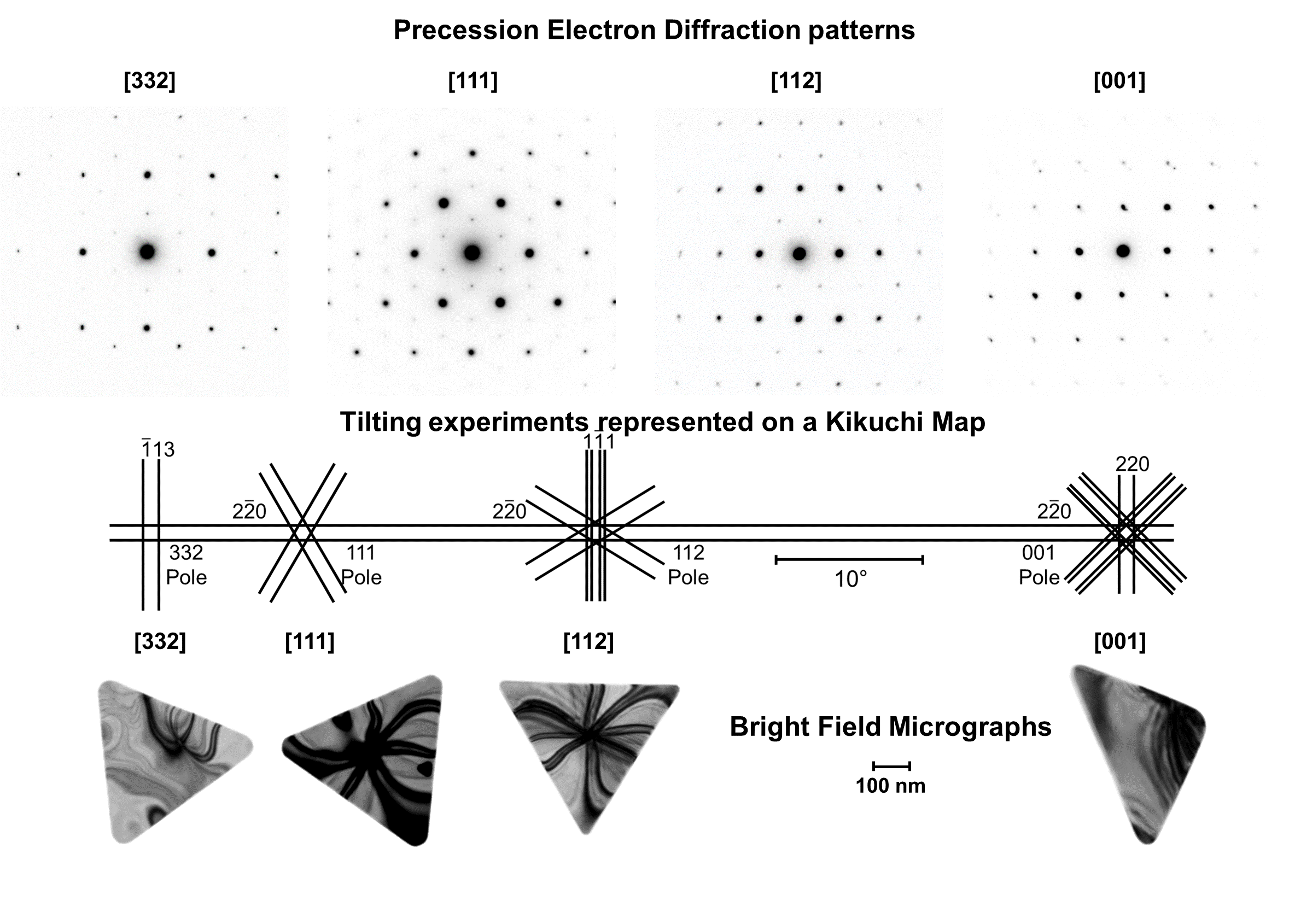
To save this page as a PDF, click this button and choose the PDF destination.

Poster Session - Physical Sciences Applications

16:00 - 16:45 Thursday, 26th November, 2020

Meeting Room 2

Track Physical Sciences Applications

Presentation type Poster Presentation


16:00 - 16:05

388 Electrochemical in situ TEM experiments with materials for solid oxide electrolysis cells

Waynah Lou Dacayan1, Christodoulos Chatzichristodoulou1, Wenjing Zhang2, Søren Bredmose Simonsen1
1DTU Energy, Kgs. Lyngby, Denmark. 2DTU Environment, Kgs. Lyngby, Denmark

Abstract Text

A high-temperature electrochemical TEM method is developed for investigation of fiber-structures. The method combines microscopy with electrochemical measurements such as I-V curves and electrochemical impedance spectroscopy (EIS). The method is applied on ceramic fibers for solid oxide electrolysis cells (SOEC).

Green energy in the form of electricity from solar and wind power can now economically outcompete electricity from fossil fuels. A combination of solar and wind power with efficient energy storage technologies, such as batteries and electrolysis cells for fuel production, will play a key role in green energy infrastructures. In particular, solid oxide electrolysis cells (SOEC) are very promising due to their exceptional conversion efficiency, but degradation processes need to be better understood and contained.

Until now, electron microscopy and electrochemical analysis of SOEC are being performed separately. This limits our access on information about the functional materials in their active state. Here, we present work where electrochemical analysis and microscopy study are combined in one experiment. We transform the TEM into an electrochemical lab for high-temperature electrochemical experiments. This is extremely challenging because it requires that hard and brittle ceramic materials are thinned to electron transparency, and that the materials are characterized during exposure to a) reactive gasses, b) electrical potentials and c) temperatures up to ca. 800 °C. In this work, electron transparency is obtained by using ceramic nanofibers prepared by electrospinning. A MEMS based heating and biasing holder is used in combination with an image-corrected ETEM to provide the combination of gas, heat and electrical polarization.

We will present images of electrode and electrolyte materials for SOEC recorded during exposure to an electrochemical environment. We will show examples of how I-V curves and EIS data can be recorded simultaneously with microscopy data, leading to a fundamental understanding of how the electrode and electrolyte materials transform as a function of variations of the parameters describing the electrochemical environment.

Acknowledgment

This project has received funding from the European Research Council (ERC) under the European Union’s Horizon 2020 research and innovation programme (grant agreement No 850850)


16:05 - 16:10

777 Analysis of Cathode-Solid Electrolyte Interfaces in Lithium-Ion Batteries using STEM

Michael Malaki1, Anuj Pokle1, Mohammad R Ahmad1, Jean Philippe Beaupain2, Katja Wätzig2, Mihails Kusnezoff2, Julian Müller3, Benjamin Butz3, Andreas Beyer1, Kerstin Volz1
1Materials Science Center (WZMW) and Faculty of Physics, Philipps University Marburg, Marburg, Germany. 2Fraunhofer Institute for Ceramic Technologies and Systems IKTS Dresden, Dresden, Germany. 3Institute of Materials Engineering, University of Siegen, 57076, Siegen, Germany

Abstract Text

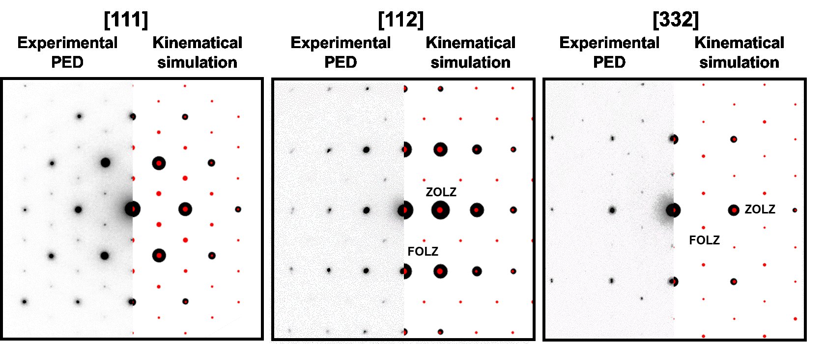
Conventional lithium-ion batteries (LIBs) make use of liquid electrolytes (LEs) to facilitate ion transport between the electrodes. However, the LEs present a significant challenge to ensure overall safety and limit the achievable energy density, which is further reduced due to the necessary separator [1]. Solid electrolytes (SEs) can circumvent these issues by playing the dual role of electrolyte and separator in combination with a cathode active material (CAM) such as the LiNi0.6Co0.2Mn0.2O2 (NCM622). The Li-ion kinetics of SE is mostly limited by its own grain boundaries and the cathode-solid electrolyte interface. The requirement of chemical compatibility of SEs with CAMs which do not degrade at high voltages led to the development of oxide SEs such as the NASICON type Li1+xAlxTi2-x(PO4)3 (LATP)  and garnet type Li7La3Zr2O12 (LLZO) compounds [2]. These are usually synthesized in powder form and sintered to get densely packed primary grains resulting in a poly-crystalline pellet. However, when combined with CAMs, poor interfacial contact between the SEs and cathodes result in high interfacial resistances [3]. SE decomposition, intermediate transition layer formation, and temperature-induced transition metal inter-diffusion during processing have been reported at micron-scale for several combinations of SE and CAMs [4]. However, direct investigation of such interfaces including grain boundaries at high spatial resolution is challenging and intimate knowledge on interfacial reactions and kinetics is lacking. 

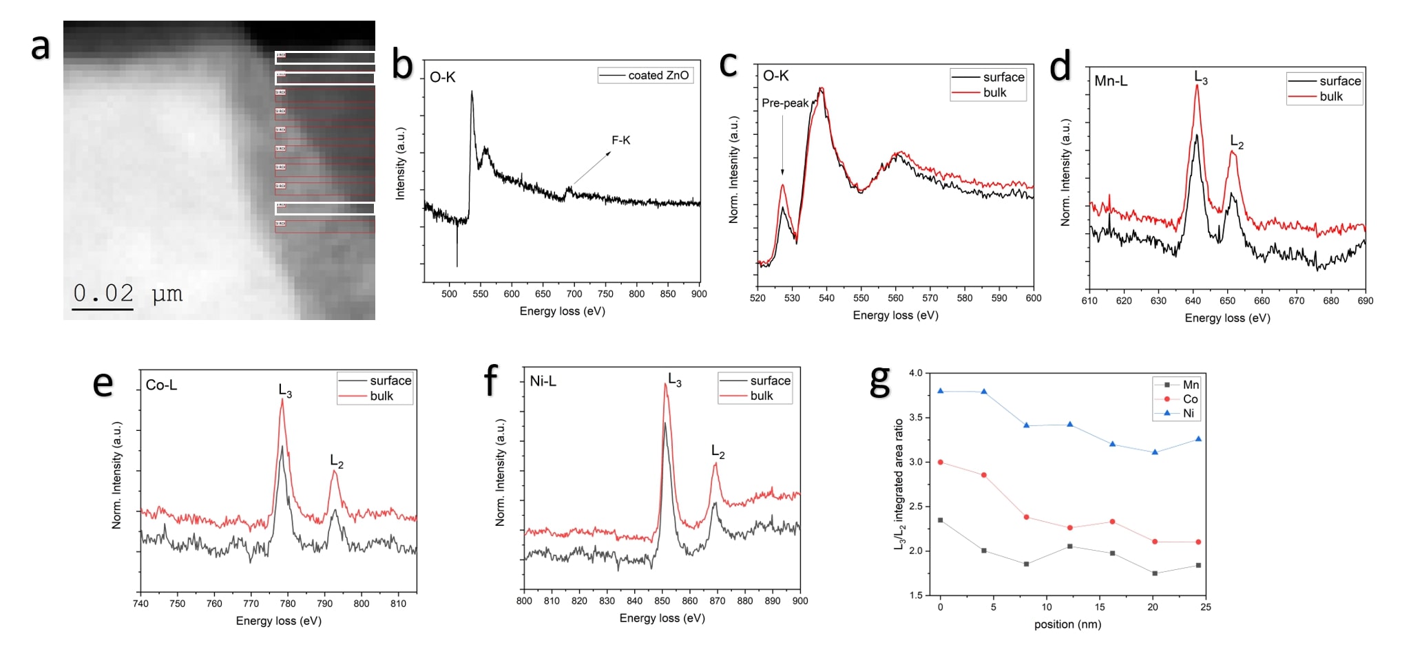
In this study, cathode-solid electrolyte composites were prepared by pressing and co-sintering NCM622 with Li1.3Al0.3Ti1.7(PO4)3 –LATP at temperatures ranging from 550-650 °C along with reference cathode and SE sintered at 650 °C respectively. Using the focused-ion beam (FIB) technique and Ar-ion nanomilling, lamellas were prepared by optimizing beam doses in order to prevent induced structural changes. Scanning transmission electron microscope (STEM) imaging in combination with electron dispersive X-ray (EDX) analysis was performed to characterize the grain boundaries and the cathode-solid electrolyte interface. In the composites, the grain morphology steadily degrades by hole formation and inter-granular cracking which was most severe at 650 °C (refer Figure 1). The transition metal inter-diffusion steadily increases with increasing sintering temperatures. We also observed transition metal segregation at the cathode grain boundaries. However, the most striking observation was the segregation of titanium (Ti) along the SE grain boundaries in a sort of core-shell structure, immediately followed by Ti-deficient regions when moving towards the center of the original LATP grains in the composites sintered at temperatures of 550 °C and 600 °C. At higher sintering temperatures, the crystal structure of the LATP completely degrades. 

The presentation will summarize the chemical composition of the LATP as well as the NCM in relation to the sintering temperature. These results help to directly visualize complex interfacial reactions that occur when cathode-solid electrolyte composites are co-sintered and to better understand the temperature influence on interface stability in order to design reliable solid-state batteries.


Uncaptioned visual

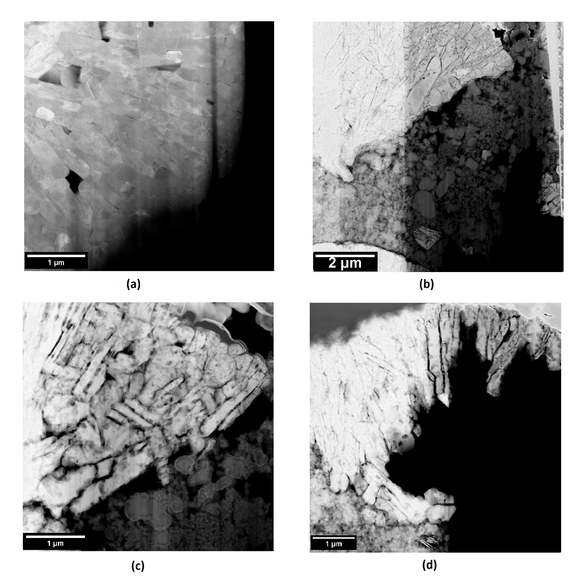
Figure 1. STEM images of (a) NCM622 reference sintered at 650 °C and NCM-LATP composites sintered at (b) 550 °C  (c) 600 °C and (d) 650 °C. The degradation of NCM grains (cracking and hole formation) is most severe in composites sintered at 650 °C.


References

[1] Nanda, J., Wang, C and Liu, P., MRS Bull. 43 (10) (2018), pp. 740–745.

[2] Nie, K. et al. Frontiers in chemistry 6 (2018), p. 616.

[3] Han, X. et al. Nature materials 16 (5) (2017), pp. 572–579.

[4] Miara, L.et al. ACS applied materials & interfaces 8 (40) (2018), pp. 26842–26850. 


16:10 - 16:15

1104 TEM study of structural and chemical evolution of coated LiNi0.6Mn0.2Co0.2O2, LiCoO2, and Si electrodes for Li-ion batteries

Ardavan Makvandi1, Martin Peterlechner1, Simone Casino2, Michael Wolff3,4, Sandra Lobe3,4, Julian Müller5, Tobias Gallasch2, Sven Uhlenbruck3,4, Martin Winter2,6, Gerhard Wilde1
1Institute of Materials Physics, University of Münster, Münster, Germany. 2MEET Battery Research Center, University of Münster, Münster, Germany. 3Institute of Energy and Climate Research, Materials Synthesis and Processing (IEK-1), Forschungszentrum Jülich GmbH, Jülich, Germany. 4Jülich Aachen Research Alliance: JARA-Energy, Jülich, Germany. 5Micro - and Nano analysis - Tomography Research Group, University of Siegen, Siegen, Germany. 6Helmholtz-Institute Münster, IEK-12, Forschungszentrum Jülich GmbH, Münster, Germany

Abstract Text

The modification of state-of-the-art electrodes by nanostructured coatings is one approach to optimize crucial battery parameters. Interfaces (e.g. active material/coating; electrode surface/electrolyte) determine the local Li-ion transport kinetics and finally the electrochemical performance. Therefore, it is necessary to study the structure and chemistry of electrodes and electrode/electrolyte interfaces. 

In this work, the structure and chemistry of the bulk and surface regions of LiNi0.6Mn0.2Co0.2O2 (NMC-622), LiCoO2 (LCO), and Si electrodes before and after electrochemical cycling were studied by transmission electron microscopy (TEM) including analytical scanning TEM (STEM). The objective of this work is to understand the effect of electrode surface and electrode/electrolyte interface on degradation mechanism and also the effect of coating layer on the stability of the electrode surface.

Al-doped ZnO coated NMC-622 powder electrode was prepared via a Microwave-assisted synthesis method. Carbon-coated silicon and Al-doped ZnO coated LCO thin film electrodes were made via magnetron sputtering and physical vapor deposition (PVD), respectively. Cross-sectionional TEM samples were prepared by FIB. Electron-energy-loss spectroscopy (EELS), energy dispersive X-ray spectroscopy (EDX), and nano-beam electron diffraction (NBD) were accomplished in STEM mode using a FEI Titan Themis G3 60-300. Additionally, high-resolution TEM (HR-TEM) was applied. 

In the case of NMC-622 and LCO electrodes, the effect of an Al-doped ZnO coating layer on the stability of the surface upon cycling was studied. In the core-loss EELS spectra, by measuring the intensity ratio (L3/L2) of L2,3-edge peaks, the oxidation states of transition metals (e.g. Ni, Mn, and Co) at surface/coating interface were quantified. 

In Fig. 1 data from a spectrum-image (SI) of high-loss EELS spectrum acquired from the coating layer are shown. Fig. 1b shows the O-K edge from Fig. 1a. In Figs. 1 c-f high-loss EELS spectra were extracted from the surface/coating interface and bulk areas of a pristine Al-doped ZnO coated NMC-622 powder electrode (the white rectangles shown in Fig. 1a) showing Ni-L3 and Co-L3 edge chemical shift to lower energy at the surface/coating interface confirming the Co and Ni oxidation state reduction at surface/coating interface compared to the bulk. Moreover, in the case of the O-K edge pre-peak, its intensity decreases at surface/coating interface compared to the bulk due to the fact that transition metals have been reduced and oxygen vacancy formation occurred. This is in line with the chemical shift of the Ni-L3 and Co-L3 edges. Moreover, the intensity ratio (L3/L2) analysis of Mn, Co and Ni, also show a Co and Ni oxidation state reduction at the surface/coating interface compared to the bulk. The length scale of detectable chemical changes is in the order of 10 nm. 

Structural changes upon a single lithiation procedure may occur on a much larger length scale, as studied on Si thin film electrodes. In Fig. 2. TEM images of a Si thin film electrode before and after a single lithiation step are shown. The volume expansion upon lithiation leads to cavities in a depth of 100 nm from the interface. The results and possible conclusions to the strategy using coating layers to improve the battery performance are discussed.


Uncaptioned visual

Fig. 1. EELS analysis of a pristine Al-doped ZnO coated NMC-622 powder electrode. (a) High-loss EELS spectrum image (SI), (b) high-loss O-K edge acquired from the coating layer shown in (a), (c-f) high-loss spectra acquired from the surface/coating interface and bulk areas (the white rectangles shown in (a)) showing Ni-L3 and Co-L3 edge chemical shift to lower energy at the surface/coating interface. Moreover, in the case of the O-K edge pre-peak, its intensity decreases at the surface/coating interface compared to the bulk (c) and the O-K edge pre-peak disappeared completely at the ZnO coating layer (b). (g) the intensity ratio (L3/L2) analysis of Mn, Co and Ni from the regions at different distances from the surface/coating interface.


Uncaptioned visual

Fig. 2. TEM images of Si thin film electrode (a) before and (b) after a single lithiation step are shown. The volume expansion upon lithiation leads to heavy changes of the solid electrolyte interface (SEI) layer on a length scale of hundreds of nm. 


16:15 - 16:20

117 Investigating zeolites implanted with single metal sites or controlled metal clusters for catalysis by advanced electron microscopy

Mr Ping-Luen Baron Ho1,2, Dr Chen Huang2, Dr Pu Zhao1, Professor Peter D. Nellist2, Professor Shik Chi Edman Tsang1
1Wolfson Catalysis Center, Department of Chemistry, University of Oxford, Oxford, United Kingdom. 2Department of Materials, University of Oxford, Oxford, United Kingdom

Abstract Text

Considerable efforts have been made to develop atomically-dispersed supported metal catalysts in order to maximize the number of catalytically active sites at a reduced metal loading. Recently, increasing attention is paid to using porous crystalline materials, e.g. zeolites and metal-organic frameworks (MOFs), as catalyst supports. Compared with conventional catalyst supports such as various metals and metal oxides, porous crystalline materials have designable topology, porosity and functionality. This work makes use of simultaneous annular dark-field imaging and ptychography in the scanning transmission electron microscope to characterise the strategic placement of defined metal catalytic active sites in the confined atom-dimensional pores of these materials, and to relate catalytic performance to the size and shape selectivity of zeolite pores, and the synergy between metal sites, Brønsted acid sites related Al/Si ratio and in the confined space.


Uncaptioned visual

Figure 1. Denoised HAADF-STEM image of ReOx/USY zeolite catalyst along the [0-11] zone axis, comparing with the raw data and FFT on right hand side. (scale bar: 3 nm)


References

[1] P. Zhao et al, J. Am. Chem. Soc. 140 (2018), 6661-6667.

[2] J.G. Lozano et al, Nano Lett., 18 (2018), 6850-6855.

[3] J. Aarons et al, Nano Lett., 17 (2017), 4003-4012.


16:30 - 16:35

658 Ceria-supported nickel catalyst for Sabatier reaction:  a detailed nanoscopy investigation

Dr Maria Chiara Spadaro1, Ms Viktoria Holovanova2, Dr Teresa Andreu2, Prof Dr Joan Ramon Morante2, Prof Dr Jordi Arbiol1
1Catalan Institute of Nanoscience and Nanotechnology (ICN2), Bellaterra (Barcelona), Spain. 2Catalonia Institute for Energy Research (IREC), Barcelona, Spain

Abstract Text

The rise of CO2 concentration in the atmosphere is considered the main challenge to mitigating global warming1. Therefore, there is an urgent need to further stimulate the society in the energy scenario transition from fuel-based to renewable carbon resources, and therefore to realise a closed-cycle carbon process: CO2 methanation through Sabatier reaction represents one of the proposed solutions.

It is important to develop advanced catalysts, with low-temperature and stable activity. Here we propose the fabrication of Ni-CeO2 catalyst by wet impregnation of mesoporous silica SBA-15 templates with cerium nitrate and nickel nitrate aqueous solutions2, 3.  The obtained sample was tested in methanation of CO2 (Sabatier reaction), proving to be highly stable, efficient and selective towards CH4

In order to address the exceptional performances observed, we performed a detailed transmission electron microscopy study in order to precisely understand their composition, the arrangement of the different chemical species and valence state variation along the nanostructure. In Figure 1 A we investigated in detail the structure of the Ni nanoparticles (NPs). As it is possible to observe in the indexed power spectrum, the Ni structure is cubic with its [1 1 1] direction parallel with respect to the electron beam. Furthermore, the (20-2) Ni plane in the [1 1 1] zone axis is almost 18º rotated with respect to the (200) ceria plane in the [0 1 0] zone axis. In Figure 1 B the core-loss EELS chemical composition maps obtained from the Ni-CeO2 structure are reported. From the relative composition analysis, reported in Figure 1 C, it is evident that the Ni present is mostly metallic (as from the comparison of the O .% and Ni .% relative maps). Furthermore, Ni nanoparticles size distribution appears to have a bimodal behaviour showing two nanoparticles size regime: (i) below 10 nm and (ii) above 20 nm. We propose that the small nanoparticles can be located both on the surface and inside the ceria mesoporous structure, while the big nanoparticles are located only on the surface of the ceria as they cannot penetrate it due to their big size. Analysing Ce M5 and M4 relative ratio, it is possible to evaluate the cerium oxidation state distribution within the sample as it is reported in Figure 1 D, observing that the ceria crystallites contain mostly Ce4+ ions. A closer look on the ceria structures is given in Figure 1 E, showing cubic fluorite CeO2 structure imaged along its [1 1 0] zone axis. Notice that most of the SBA channels follow the same orientation with slight axial tilts of ±10º. The area evidenced in the yellow box grow along the same axis as the previous structure, and here it is possible to highlight the termination of these nanostructures showing that those expose mainly {1 1 1} and {0 0 1} family of planes. In order to highlight the common axis/orientation of the different SBA-15 channels and to quantify the corresponding crystal rotation we performed geometrical phase analysis (GPA) taking as reference the frequency corresponding to the (-1 1 1) direction, as reported in Figure 1 E (bottom). Additionally, electron tomography experiments are planned to reconstruct the 3D structure of Ni-CeO2 and to investigate Ni nanoparticles distribution within the mesoporous structure.

Uncaptioned visual

Figure 1 (A) HRTEM image of Ni nanoparticle on the ceria mesoporous structure together with the blow up in the Ni nanoparticle area and its corresponding indexed power spectrum. In the bottom a frequency filtered map evidencing Ni and CeO2 planes is also reported.  (B) HAADF STEM image of the sample and STEM-EELS elemental maps obtained on the selected areas as indicated in the white box. The maps shown in the Spectrum Images have been obtained by using: O k-edge at 532 eV (green), Ni L-edge at 855 eV (red) and Ce M-edge at 883 eV (blue), as well as composites of O-Ni-Ce. Scale bar in the maps equal to 20 nm. (C) Relative intensity maps of the different elements. (D) Ce M5/M4 intensity ratio map is also reported. (E) HRTEM image of the Ni-ceria structure. In the yellow panel the blow-up of the ceria SBA-15 edge is highlighted evidencing the exposed planes. The power spectrum of the full image (red box) and GPA rotation map are also reported. 


References

  1. Raphael Neukom et al. Nature 2019, 571, 550.
  2. Andreina Alarcón et al. Applied Catalysis B: Environmental 2020, 263, 118346.
  3. Jordi Arbiol et al. Applied Physics Letters 2002, 81 (18), 3449.

16:35 - 16:40

669 Nanoplate’s crystallography: A full description using pseudo-kinematical electron diffraction

Ms Miriam Carolina Mendoza-Ramirez, Professor Miguel Avalos-Borja
Instituto Potosino de Investigación Científica y Tecnológica A. C., San Luis Potosí, Mexico

Abstract Text

Summary

Discussion on plate nanoparticle´s (NP) forbidden reflections (FR) have prevailed for at least 40 years, [1] partly due to the “dynamical effects” present on Selected Area Electron Diffraction (SAED) has hindered NP´s fine structure determination. On this work the use of Precession Electron Diffraction technique (PED) [2] have had a pivotal role on describing novel aspects of these particles complementing and extending the understanding of Au triangular nanoparticles structure.

Introduction

Au nanoplates have several applications on different fields as Surface-Enhanced Raman Spectroscopy (SERS), photovoltaics, molecular detection or photothermal cancer therapies. Plate’s properties can be determined by either, size, shape or structural defects. The last property is typically characterized by SAED, due to nanoparticles characteristics dimensions.[3] However, this technique is often affected by the dynamic diffraction effect, producing FR and giving useless (for fine structure determination) ED patterns in most cases.

Nanoplates have been distinguished due to the 1/3{422} FR which have been “explained” by several models, such as stacking faults, [4] twins or thickness effects. [5][6] Unfortunately these models have not been verified, mainly because there are no experiments with the ability to study these particles three-dimensionally.

On this work, recent advances on the full nanoplate’s crystallographic description are presented. Relevant highlights from this research are that Au nanoplates were three-dimensionally studied in two aspects, morphology (front and side view) and structure. Several improvements on nanoplate’s characterization were obtained by using the PED technique and the tridimensional cell parameters for a novel hexagonal Au unit cell (Auhex) will be presented. The lattice parameters for this phase were determined using kinematical experimental data. Additionally, this work discusses and dismisses those models which are inconsistent with our experimental results. A model considering “two phases” is proposed and corroborated by using kinematical simulation. According to this model it was found that there are two phases involved (Aufcc and Auhex), which keep specific crystallographic orientation relationships. 

Materials and methods

Nanoplate’s syntheses procedure: Au NP´s were synthetized according to a well-known published polyol process. [7]

TEM characterizations: TEM samples were prepared by diluting samples in isopropyl alcohol and mounted on Cu grids. Bright field (BF) Characterizations were achieved using a FEI Tecnai-F30 TEM at 300 kV. NP were oriented by using a double tilt sample holder. For PED acquisition a Spinning Star P-20® PED unit was used, with a precession angle of 2.4°. Micrographs were acquired by using a Gatan® Orius SC200 digital camera. Digital Micrograph® and Mac Tempas® software were used for micrograph treatment and kinematical diffraction simulation, respectively.

Results and Discussion

Polyol synthesis produces a great variety of products (rods, wires, decahedrons, tetrahedrons, etc.). However, this study was focused only on triangular plates like those shown on Figure 1. 

For acquiring information on the particle´s three dimensions several tilting experiments like those shown on Figure 1 were done. Nanoplates in this figure exhibit diffraction contrast as bending contours in image mode. This contrast can be directly related with nanoparticle´s orientation. As can be seen in Figure 1, this experiments were obtained tilting around the [1-10] direction, covering an angular space of more than 60 degrees. Nevertheless, for several experiments it was also possible to acquire nanoplate´s Zone Axis Patterns (ZAP) on side view, making plate’s three dimensional characterization possible.

In terms of diffraction, the PED technique enables to obtain patterns that look perfectly oriented and with minimized dynamical diffraction effects (intensity profiles will be properly discussed on poster presentation). Patterns presented on this abstract were indexed according to a cubic FCC phase, but in all of them it is possible to note FR´s as can be observed in the patterns of Figures 1 and 2.


Uncaptioned visual

Figure 1. Typical experiments on which nanoplates were tilted away from [111] zone axis.


By studying symmetry and spot position in all obtained patterns, several assertions were proposed. The first observation is that 1/3{422} FR are not really produced by double diffraction, otherwise, their intensity would have been dramatically minimized by the use of the PED technique, therefore these spots are most likely produced by stacked fault planes and are not forbidden by space group symmetry. The second proposed statement, implies the existence of two diffracting lattices. One is a perfect cubic crystal and the second is a hexagonal crystal whose lattice parameters were measured directly on ZAP+ PED patterns.

For describing experimental results a model which included two gold phases was besought. The first phase in this model is the well-known Au structure, exhibiting strong diffraction spots and the second one is a hexagonal structure which has a weaker intensity due to the fact that diffracted spots arise from only a few atomic layers.


Uncaptioned visual

Figure 2. Kinematical simulations are shown for three experimental patterns.

To verify experimental results (as those in Fig. 2) we simulated kinematical diffraction patterns assuming for Aufcc the typical No. 225 space group and for Auhex the hexagonal No. 174 space group structure. For these two phases a specific orientation relationship was fixed. For several directions, the hexagonal phase was so thin that ZOLZ and FOLZ could be found on simulation, reproducing all experimental patterns. 

Conclusion

PED characterizations prove to have better precision than those performed using SAED for characterizing nanoplates. A “two phase model” was able to reproduce experimental patterns on more than eight different zone axis diffraction patterns in TNP.[8]


References

[1]       K. Heinemann, et al., J. Cryst. Growth, 47(2),177–186, 1979.

[2]       R.Vincent. and P.A.Midgley, Ultramicroscopy, 53 (3), 271–282, 1994.

[3]       J. E. Millstone, et al., Small, 5(6), 646–664, 2009.

[4]       V. Germain, et al., J. Phys. Chem. B, 107(34), 8717–8720, 2003.

[5]       A. I. Kirkland, et al., R. Soc., 440, 589–609, 1993.

[6]       J. Reyes-Gasga, et al., Ultramicroscopy, 108 (9), 929–936, 2008.

[7]       C. Kan et al., J. Nanomater., 2010, 1–9, 2010.

[8]       We thank the LINAN laboratories, Hector Silva-Pereyra and Lucia Aldana-Navarro.